Diode and Power Conversion System
a power conversion system and diode technology, applied in the direction of basic electric elements, electrical equipment, semiconductor devices, etc., can solve the problems of increasing recovery loss, unable to efficiently annihilate the electrons and holes remaining on the cathode electrode side in the n-type cathode layer 1 at the time of recovery,
- Summary
- Abstract
- Description
- Claims
- Application Information
AI Technical Summary
Benefits of technology
Problems solved by technology
Method used
Image

Examples
first embodiment
[Structure of Diode]
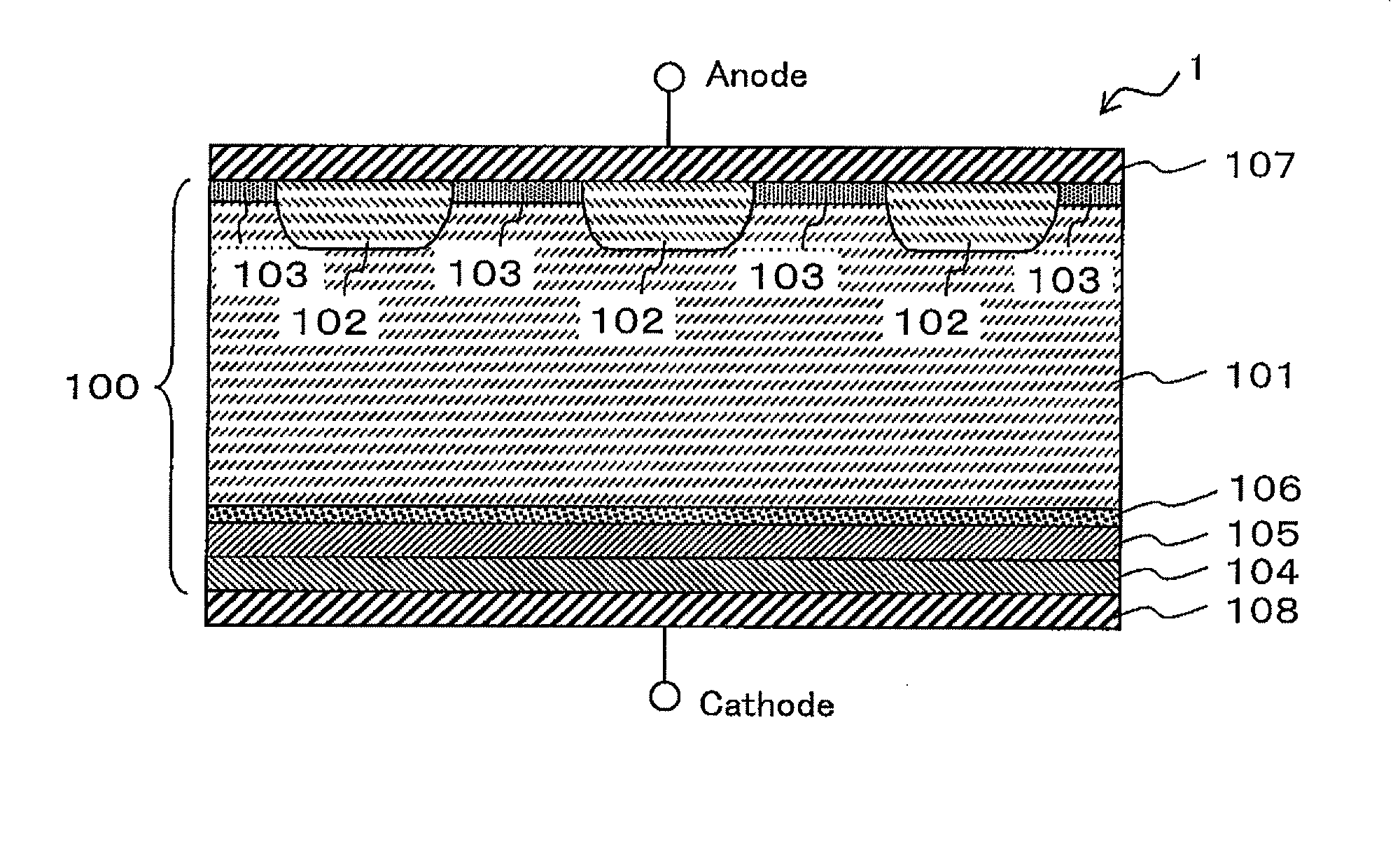
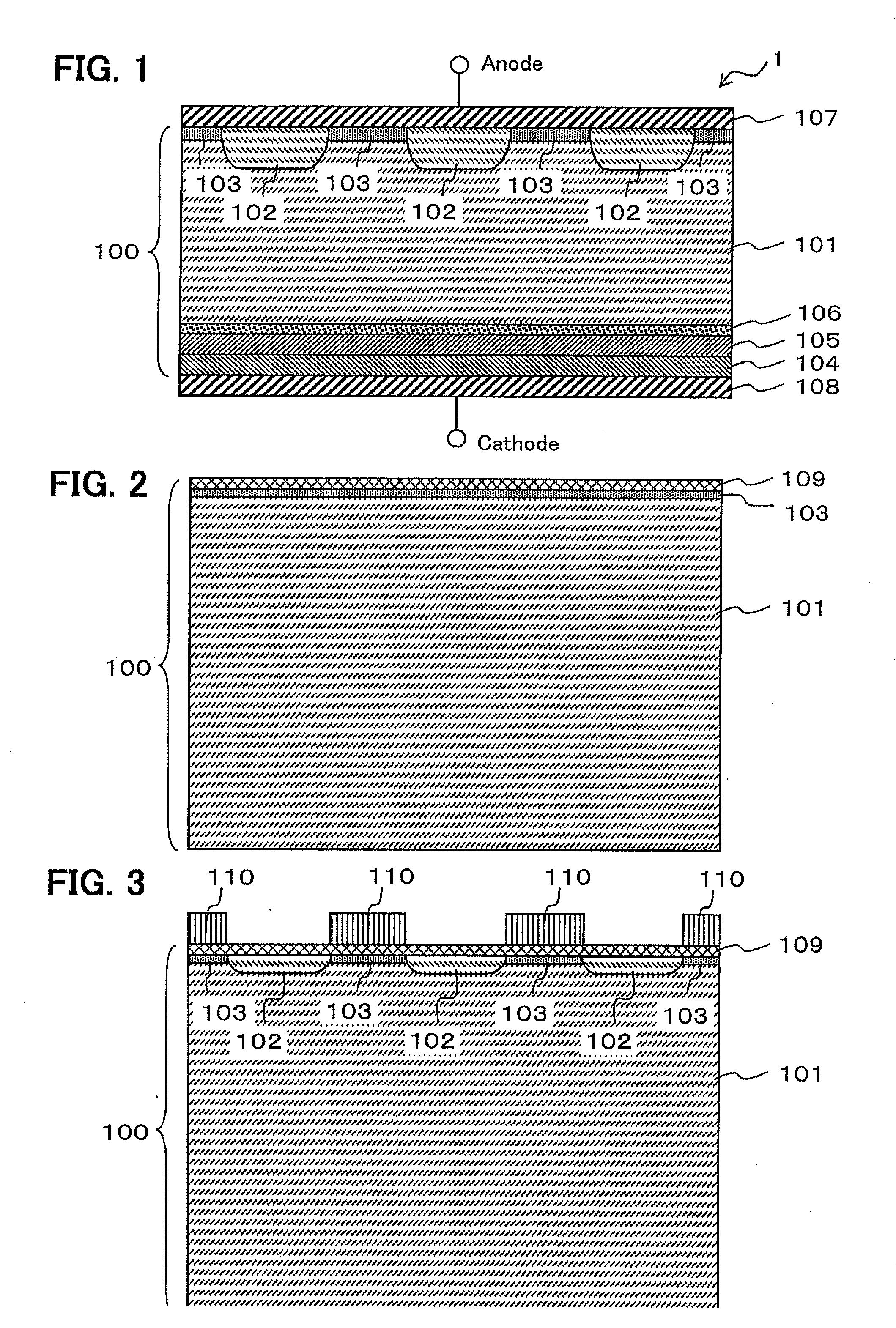
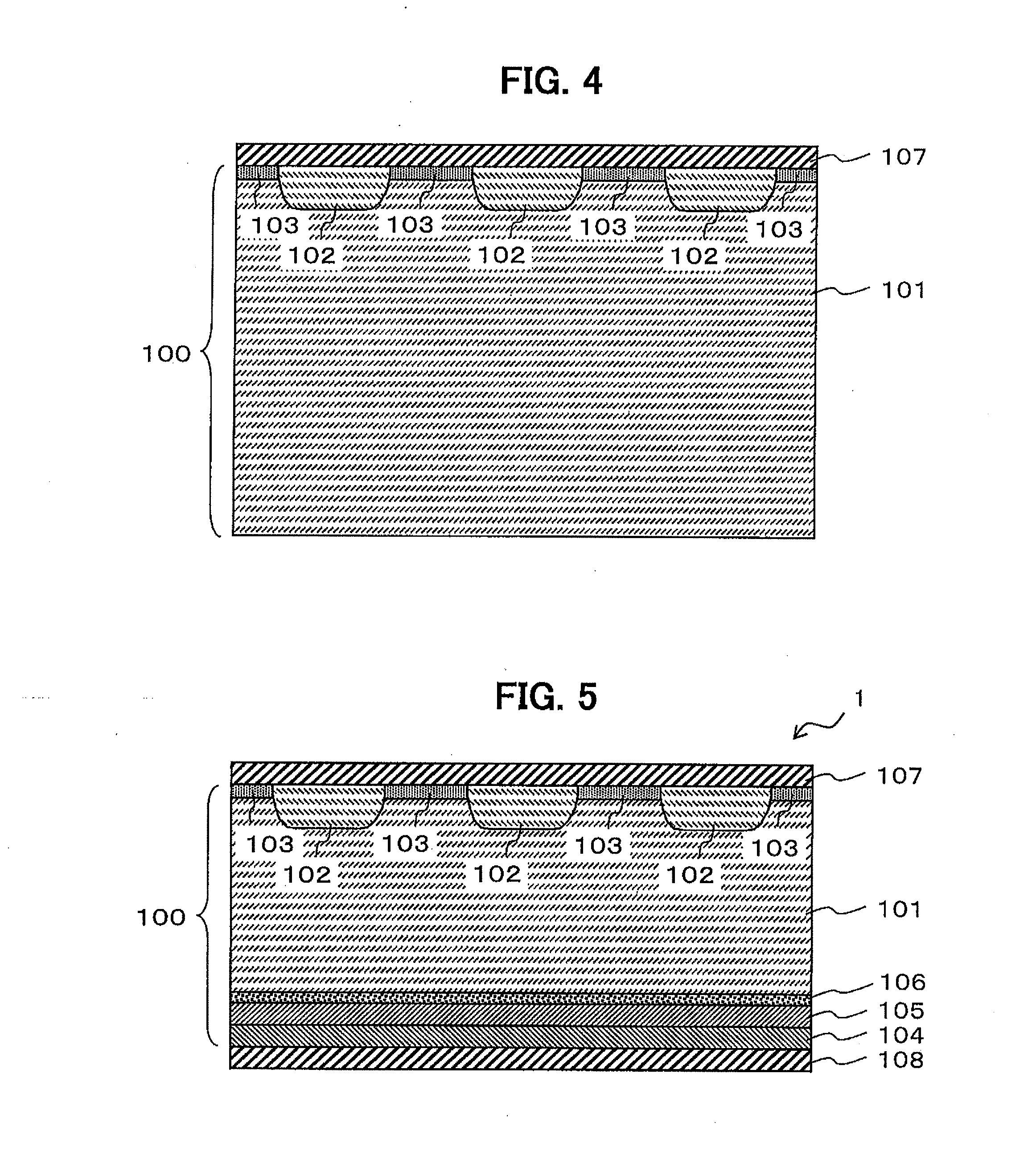
[0044]The structure of the diode according to the first embodiment of the present invention is explained below with reference to FIG. 1, which is a schematic cross-sectional view of the active region of the diode according to the first embodiment of the present invention. Although not shown, a conventional termination structure such as an FLR (field limiting ring) structure is used in the termination region. In the FLR structure, a p-type well and an electrode are arranged in a circular arrangement.
[0045]As illustrated in FIG. 1, the diode 1 according to the first embodiment is includes an n− drift layer 101, an anode p layer 102, an anode p− layer 103, a cathode n layer 104, a cathode buffer n layer 105, a low-lifetime region layer 106, an anode electrode 107, and a cathode electrode 108.
[0046]In the following explanations, the entire semiconductor layered portion in each stage in the process for manufacturing the diode may be referred to as the Si substrate 100...
second embodiment
[0104]Next, the structure of the diode according to the second embodiment according to the present invention is explained below with reference to FIG. 7. FIG. 7 is a schematic cross-sectional view of the active region of the diode 1A according to the second embodiment. Although the termination region is not shown, similarly to the first embodiment, a conventional termination structure such as an FLR (field limiting ring) structure is used in the termination region. In the FLR structure, a p-type well and an electrode are arranged in a circular arrangement.
[0105]As illustrated in FIG. 7, the diode 1A according to the second embodiment is different from the diode 1 according to the first embodiment (illustrated in FIG. 1) in that the anode p layer 102 (corresponding to the aforementioned second semiconductor layer) does not have a well structure and is formed over the entire anode-side surface of the active region without arranging the anode p− layer 103. The structure of the other po...
third embodiment
3. Third Embodiment
[0107]Next, the structure of the diode according to the third embodiment according to the present invention is explained below with reference to FIG. 8. FIG. 8 is a schematic cross-sectional view of the active region of the diode 1B according to the third embodiment. Although the termination region is not shown, similarly to the first and second embodiments, a conventional termination structure such as an FLR (field limiting ring) structure is used in the termination region. In the FLR structure, a p-type well and an electrode are arranged in a circular arrangement.
[0108]As illustrated in FIG. 8, the diode 1B according to the third embodiment is different from the diode 1A according to the second embodiment (illustrated in FIG. 7) in that the cathode buffer n layer 105 is not arranged, and the low-lifetime region layer 106 (the fourth semiconductor layer) is arranged in a position adjoining to the n− drift layer 101 side (the first semiconductor layer side) of the...
PUM
 Abstract
Description
Claims
Application Information
 - R&D
- Intellectual Property
- Life Sciences
- Materials
- Tech Scout
- Unparalleled Data Quality
- Higher Quality Content
- 60% Fewer Hallucinations
Browse by: Latest US Patents, China's latest patents, Technical Efficacy Thesaurus, Application Domain, Technology Topic, Popular Technical Reports.
© 2025 PatSnap. All rights reserved.Legal|Privacy policy|Modern Slavery Act Transparency Statement|Sitemap|About US| Contact US: help@patsnap.com