Local write and read assist circuitry for memory device

a memory device and assist circuit technology, applied in the field of memory devices, can solve the problems of dwindling the scaling of the 8t sram cell, increasing the overhead increasing the size of the read stack transistor, so as to achieve the effect of further reducing the power consumption of the write operation

Active Publication Date: 2014-03-13
STICHTING IMEC NEDERLAND +1
View PDF6 Cites 9 Cited by
  • Summary
  • Abstract
  • Description
  • Claims
  • Application Information

AI Technical Summary

Benefits of technology

[0012]It is a first aim of the present disclosure to provide a memory device and / or a method for writing a cell of a memory device, with which power consumption during write operations can be further reduced.

Problems solved by technology

Read-decoupled 8T SRAM cells offer a higher degree of variability resilience compared to 6T SRAM cells, but at the expense of an increased area overhead.
Therefore, comparison of the 8T SRAM cell at the constant value of read current could result in an increased size of READ stack transistors, thereby dwindling the scaling of the 8T SRAM cell.
Thirdly the low swing bit-line (global write bit lines) reduces the READ energy consumption but the WRITE energy consumption is not optimized as the WRITE operation requires full voltage swing on the local write bit-lines of an accessed SRAM cell.
Therefore WRITE energy consumption is more critical than the READ energy consumption and is a vital issue for realizing ultra low energy SRAMs.
Further reduction of the voltage swing on the highly capacitive bit-lines is limited by the degraded WM for the scaled technologies at the lower voltages.
In addition to the area overhead of SAC-SRAM, the GND connection via NMOS transistor degrades the read static noise margin (SNM) and reduces the cell read current.
The presence of local sense amplifier as a local write assist in memory requires complex memory matrix optimization and also the area overhead is high.
However the complex memory matrix optimization, the increasing mismatch offset of the local write receiver and the increased timing complexity are left unaddressed.
This directly translates into increased energy consumption and the area penalty of the local write receiver.
Secondly, the traditional strobed local write receiver requires several critical timing signals that must be applied in a sequential order with sufficient margins.
This requires an expensive timing circuitry and also introduces significant timing margins thereby increasing the access time.
Process variations can easily lead to write failures either due to sensing failure of the local write receiver or because of the degraded write-ability of the accessed SRAM cell.
The impact of transistor sizing in improving write-ability can be very prominent at the high supply voltage levels but at the low supply voltage levels the impact of transistor sizing can be very limited in advanced CMOS technologies.
But at the same time the added power consumption and area overhead is an equally important parameter.
Use of more than one assist technique not only increases the design complexity but also results in an increased area and power consumption overhead.
The read current Iread is severely impacted by the increased process variations with technology scaling.
The presence of the logic gates not only increases area but also results in complex memory matrix optimization.
However, achieving the same benefit from the logic circuit is difficult because the logic circuit layout tends to be irregular.
As a result the conventional logic circuit based local assist techniques complicate the litho optimization of the memory matrix.
Enforcing shape-level regularity for litho optimization is a difficult task with the existing conventional local assist techniques.

Method used


Image

  • Local write and read assist circuitry for memory device
  • Local write and read assist circuitry for memory device
  • Local write and read assist circuitry for memory device

Examples


Embodiment Construction

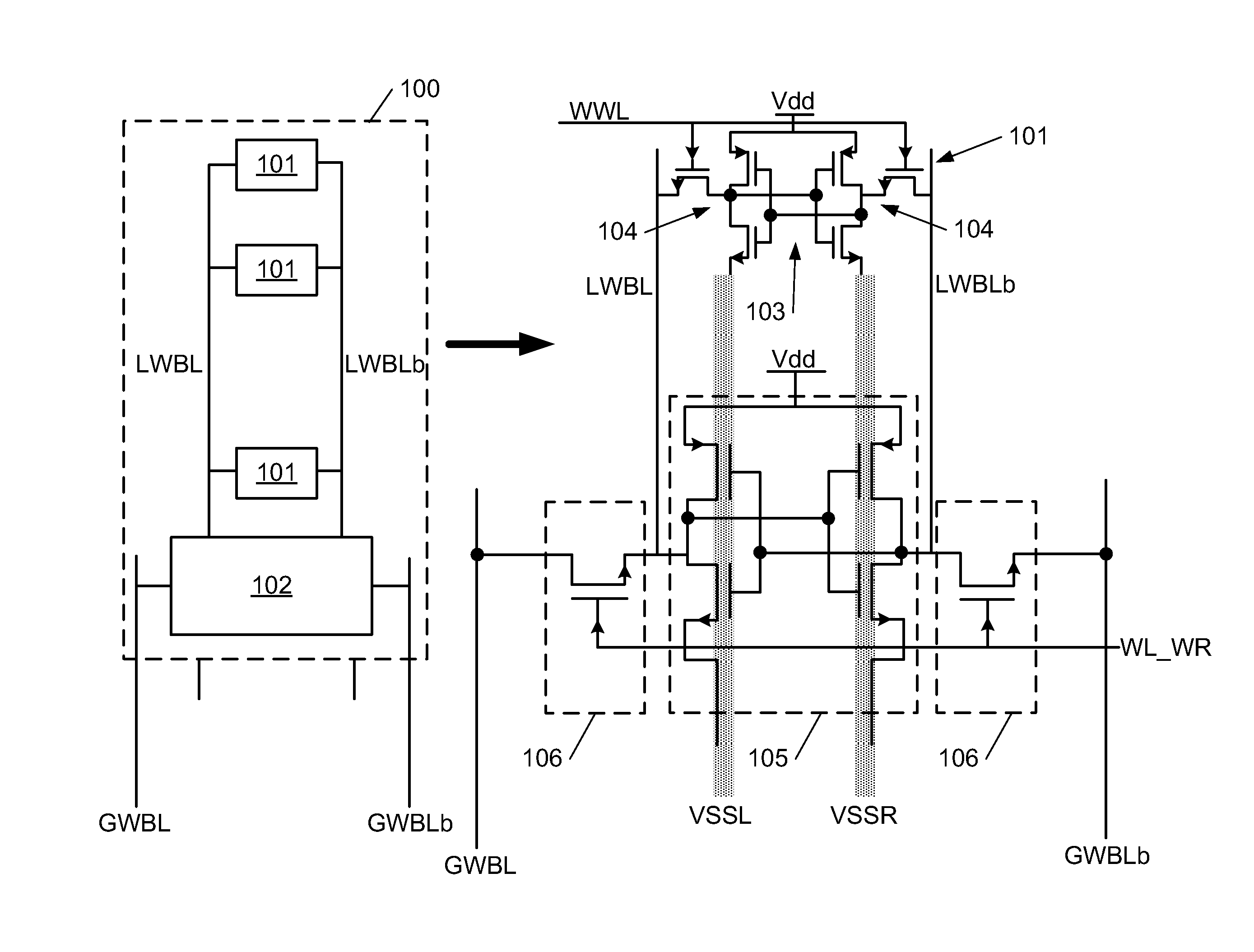
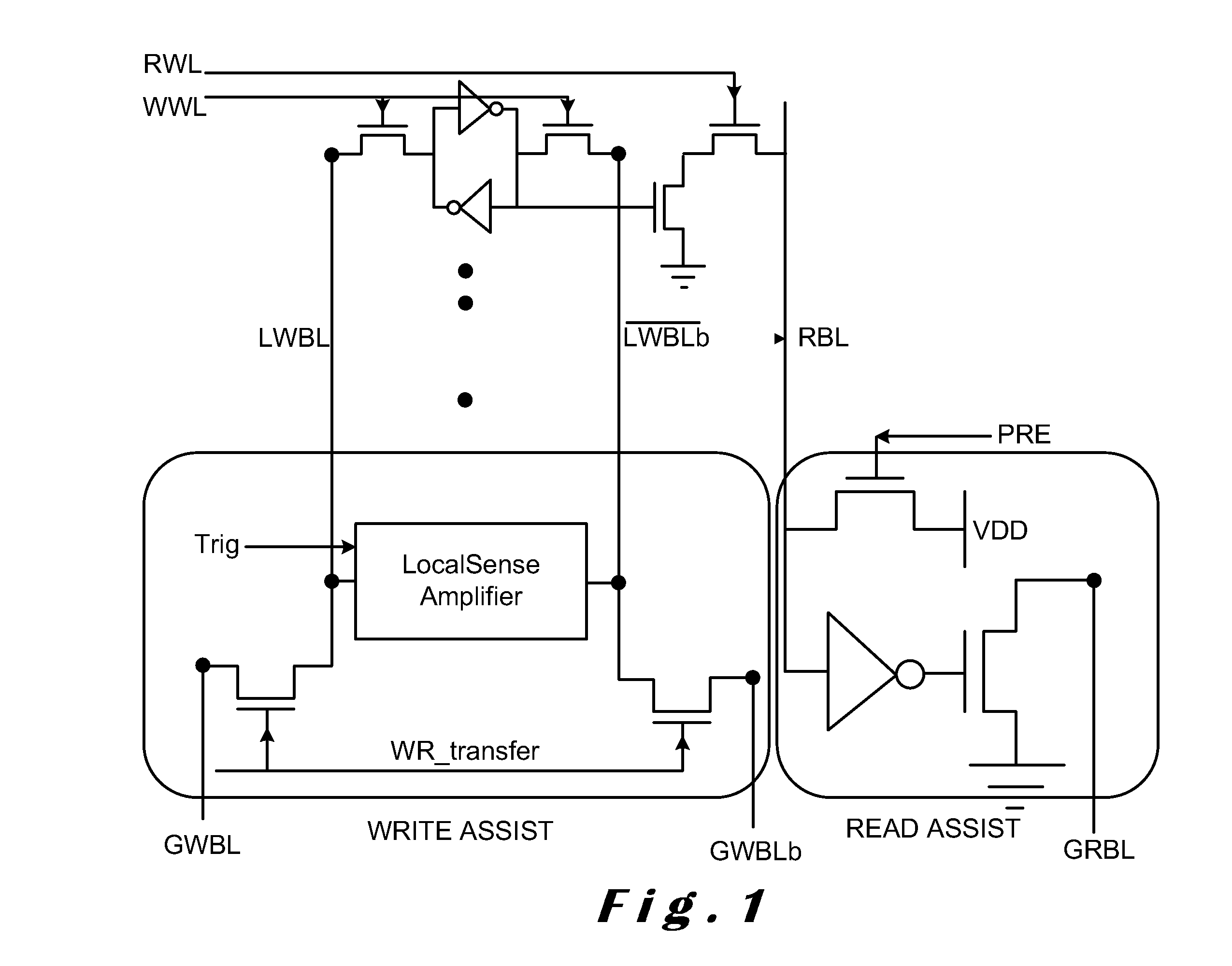
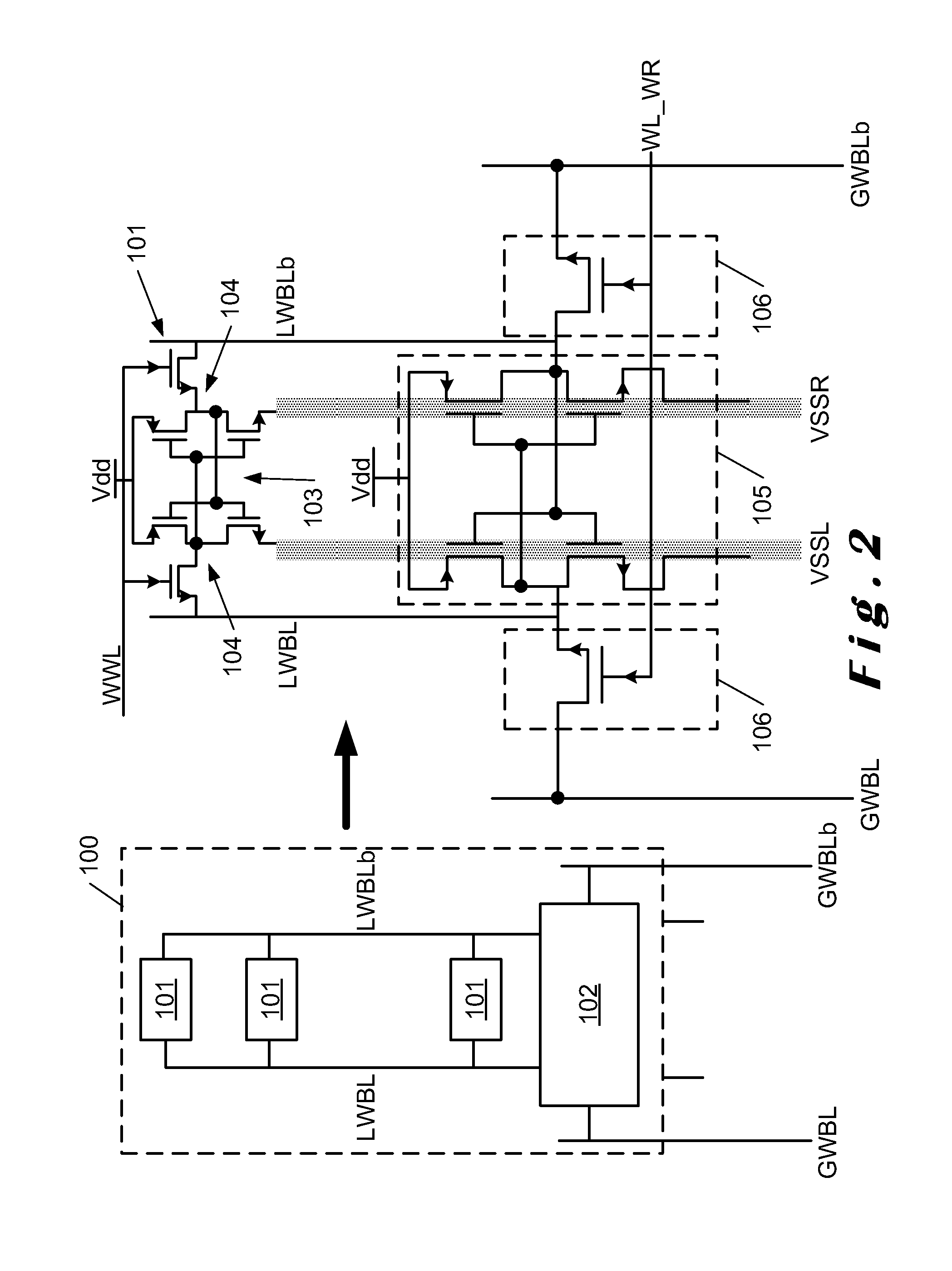
[0044]The present disclosure will be described with respect to particular embodiments and with reference to certain drawings but the disclosure is not limited thereto but only by the claims. The drawings described are only schematic and are non-limiting. In the drawings, the size of some of the elements may be exaggerated and not drawn to scale for illustrative purposes. The dimensions and the relative dimensions do not necessarily correspond to actual reductions to practice of the disclosure.

[0045]Furthermore, the terms first, second, third and the like in the description and in the claims, are used for distinguishing between similar elements and not necessarily for describing a sequential or chronological order. The terms are interchangeable under appropriate circumstances and the embodiments of the disclosure can operate in other sequences than described or illustrated herein.

[0046]Moreover, the terms top, bottom, over, under and the like in the description and the claims are use...


PUM


Abstract

A memory device having complementary global and local bit-lines, the complementary local bit-lines being connectable to the complementary global bit-lines by means of a local write receiver which is configured for creating a full voltage swing on the complementary local bit lines from a reduced voltage swing on the complementary global bit lines. The local write receiver comprises a connection mechanism for connecting the local to the global bit-lines and a pair of cross-coupled inverters directly connected to the complementary local bit lines for converting the reduced voltage swing to the full voltage swing on the complementary local bit lines.

Description

INCORPORATION BY REFERENCE TO ANY PRIORITY APPLICATIONS[0001]Any and all applications for which a foreign or domestic priority claim is identified in the Application Data Sheet as filed with the present application are hereby incorporated by reference under 37 C.F.R. §1.57. This application is a continuation of PCT Application No. PCT / EP2012 / 053757, filed Mar. 5, 2012, which claims priority under 35 U.S.C. §119(e) to U.S. Provisional Patent Application No. 61 / 449,425, filed Mar. 4, 2011. Each of the above applications is incorporated herein by reference in its entirety.BACKGROUND[0002]1. Field[0003]The present disclosure relates to memory devices, e.g. static random access memory devices, in particular local write and read assist circuitry for memory devices, and to electronic devices comprising these memory devices.[0004]The present disclosure further relates to a method for writing a cell of a memory device, e.g. a static random access memory device.[0005]2. Description of the Rel...

Claims


Application Information

Patent Timeline
Patent Type & Authority Applications(United States)
IPC IPC(8): G11C11/419
CPCG11C11/419G11C7/18G11C11/412
Inventor SHARMA, VIBHUCOSEMANS, STEFANDEHAENE, WIMCATTHOOR, FRANCKYASHOUEI, MARYAMHUISKEN, JOS
Owner STICHTING IMEC NEDERLAND
Why Eureka
Try Eureka