
Semiconductor structure

a technology of semiconductors and structures, applied in the direction of semiconductor devices, electrical equipment, transistors, etc., can solve the problems of large electric field gradient, difficult to fill the recess or trench structure, and difficult to implant in the sidewall, so as to improve the electrical properties of gate devices formed by this method

Active Publication Date: 2014-03-20
UNITED MICROELECTRONICS CORP
View PDF11 Cites 20 Cited by
  • Summary
  • Abstract
  • Description
  • Claims
  • Application Information

AI Technical Summary

Benefits of technology

This approach enables precise control of doping concentration and profile, reduces parasitic capacitance, and improves the electrical properties of gate devices by overcoming spacer-related issues in conventional fin FET fabrication.

Problems solved by technology

The material of said spacer tends to remain on the sidewalls of the fin structure, and the poor gap filling capacity makes it hard to fill the recess or the trench structure during the formation of said spacer.
Furthermore, the presence of a spacer will hinder the following ion implantation process for forming lightly doped drain (LDD), because the dopants will be blocked by the spacer and will be hard to be implanted in the sidewalls of the fin structures.
Thus, the gate device formed by this conventional process may induce a large electric field gradient and impact the electrical properties of the gate device.

Method used


Image

  • Semiconductor structure
  • Semiconductor structure
  • Semiconductor structure

Examples


Embodiment Construction

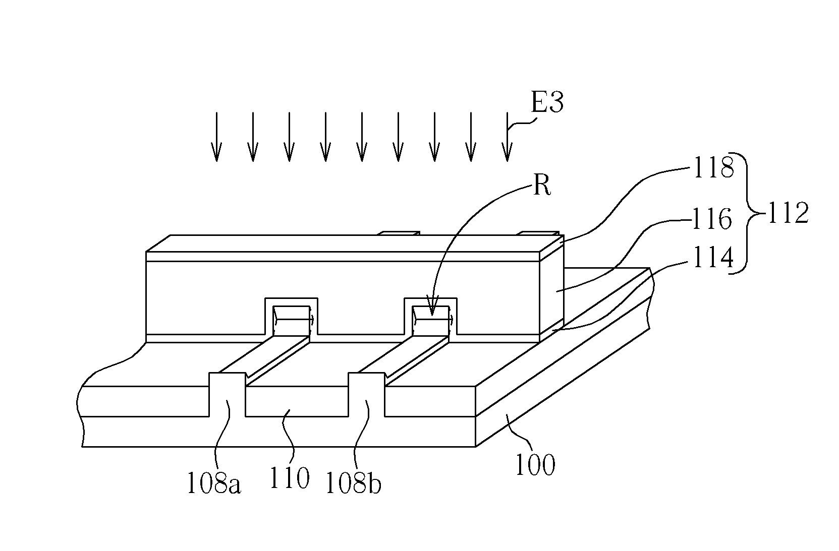
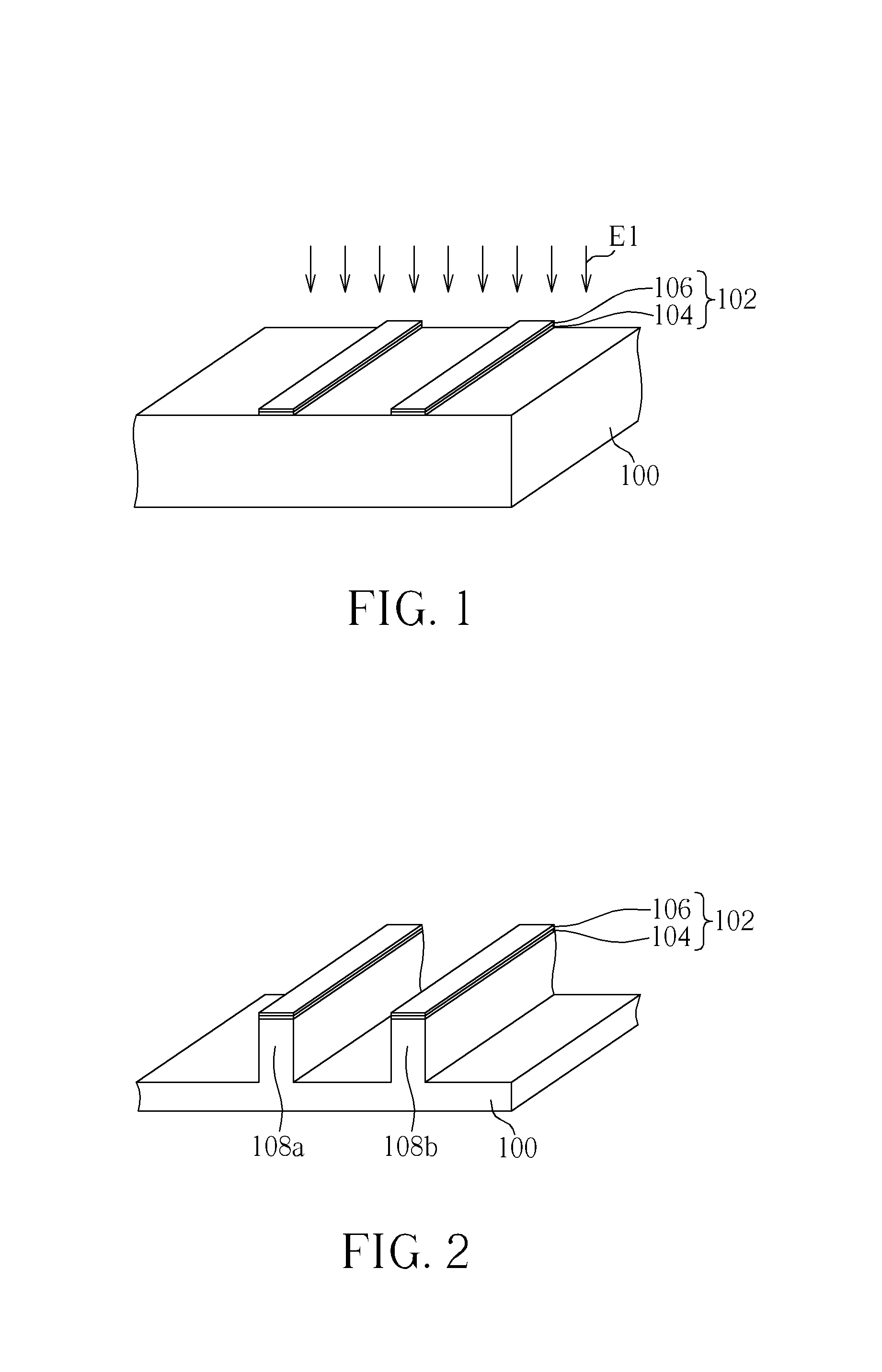
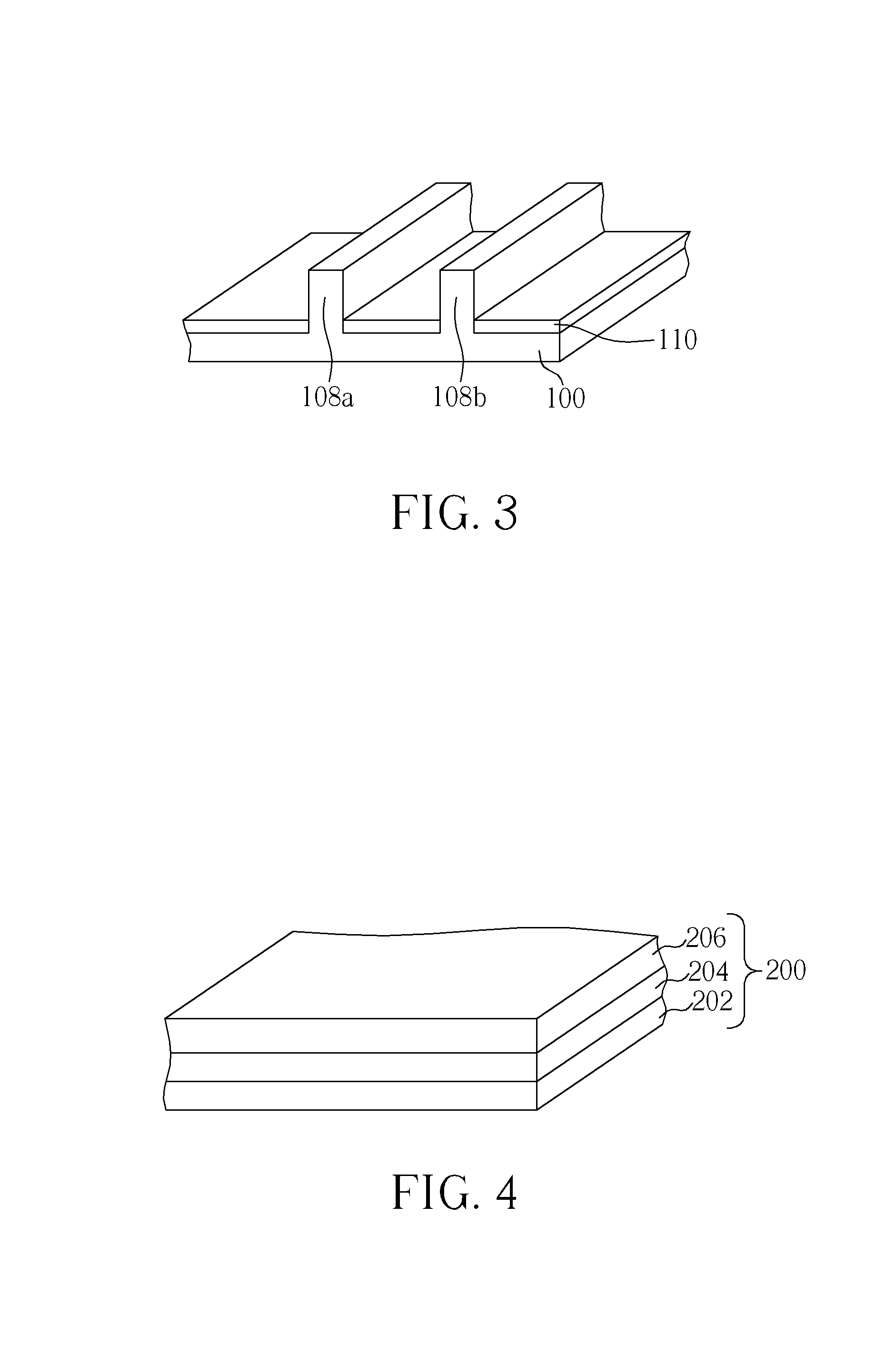
[0018]The embodiments will now be explained with reference to the accompanying drawings to provide a better understanding of the process of the present invention, wherein FIGS. 1-14 are cross-sectional views illustrating the flow of a non-planar semiconductor process in accordance with one embodiment of the present invention; FIG. 15 is a prospective view illustrating the gate device formed by the process of the present invention; FIGS. 16-21 are cross-sectional views illustrating the flow of a planar semiconductor process in accordance with another embodiment of the present invention; and FIGS. 22-25 are cross-sectional views illustrating the flow of a replacement metal gate (RMG) process in accordance with one further embodiment of the present invention.

[0019]First, please refer to FIGS. 1-15. Those figures illustrate sequentially the flow of a non-planar semiconductor process. The non-planar semiconductor process of the present invention comprises fabricating a fin field-effect t...


PUM

PropertyMeasurementUnit
heightaaaaaaaaaa
heightaaaaaaaaaa
overlapping areaaaaaaaaaaa

Abstract

A non-planar semiconductor structure comprises a substrate, at least one fin structure on the substrate, a gate covering parts of the fin structures and part of the substrate such that the fin structure is divided into a channel region stacking with the gate and source / drain region at both sides of the gate, a plurality of epitaxial structures covering on the source / drain region of the fin structures, a recess is provided between the channel region of the fin structure and the epitaxial structure, and a spacer formed on the sidewalls of the gate and the epitaxial structures, wherein the portion of the spacer filling in the recesses is flush with the top surface of the epitaxial structures.

Description

CROSS REFERENCE TO RELATED APPLICATIONS[0001]This application is a divisional of application Ser. No. 13 / 367,382 filed Feb. 7, 2012, and included herein by reference.BACKGROUND OF THE INVENTION[0002]1. Field of the Invention[0003]The present invention relates generally to a semiconductor device. In particular, the present invention relates to a semiconductor device with a pull backed gate structure.[0004]2. Description of the Prior Art[0005]In recent years, as various kinds of consumer electronic products are constantly improved and miniaturized, the size of semiconductor components have reduced accordingly, in order to meet the requirement of high integration, high performance, and low power consumption.[0006]With the trend in the industry being towards scaling down the size of the metal oxide semiconductor transistors (MOS), three-dimensional or non-planar transistor technology, such as fin field effect transistor technology (Fin FET) has been developed to replace planar MOS trans...

Claims


Application Information

Patent Timeline
Patent Type & Authority Applications(United States)
IPC IPC(8): H01L29/78H01L29/786
CPCH01L29/7834H01L29/78654H01L29/785H01L29/66795
Inventor LIU, AN-CHILIN, CHUN-HSIENTUNG, YU-CHENGLIN, CHIEN-TINGCHIANG, WEN-TAITSAI, SHIH-HUNGFU, SSU-ICHEN, YING-TSUNGCHEN, CHIH-WEI
Owner UNITED MICROELECTRONICS CORP
Learn More