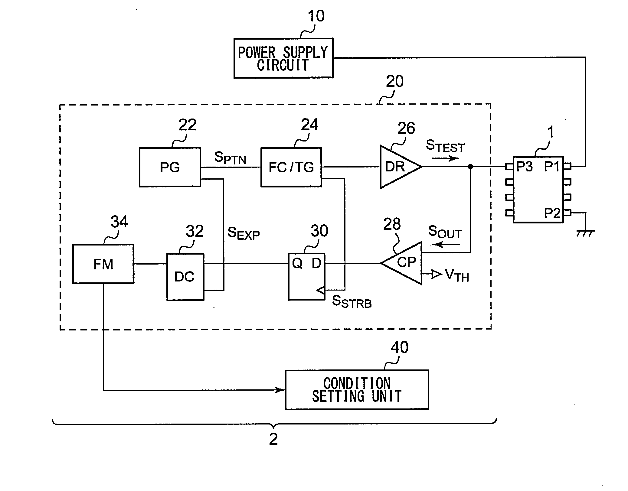
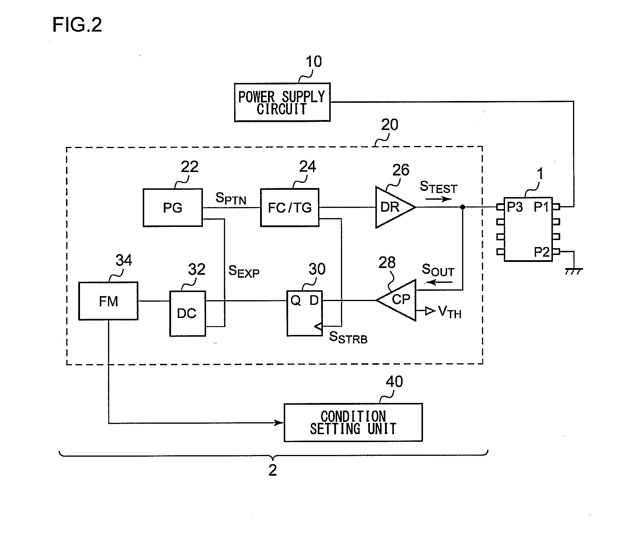
Test apparatus

a test apparatus and test tube technology, applied in the direction of testing circuits, semiconductor/solid-state device testing/measurement, instruments, etc., can solve the problem of not negligible output impedance of circuits, and achieve the effect of reducing divergence in test results

Active Publication Date: 2014-04-03
THE UNIV OF TOKYO +1
View PDF6 Cites 6 Cited by
  • Summary
  • Abstract
  • Description
  • Claims
  • Application Information

AI Technical Summary

Benefits of technology

[0012]The present invention has been made in order to solve such a problem. Accordingly, it is an exemplary purpose of an embodiment of the present invention to provide a test apparatus and test method configured to be capable of reducing divergence in the test results.
[0014]With such an embodiment, by measuring the first device characteristic value and the second device characteristic value, such an arrangement is capable of determining the test conditions with high precision. Furthermore, by performing the main test using the test conditions determined by the condition setting unit, such an arrangement is capable of reducing divergence in the test results of the user environment and the tester environment.

Problems solved by technology

Also, various kinds of analog circuits and various kinds of analog / digital hybrid circuits also have a problem of such a fluctuation in the operating current.
However, in actuality, such a power supply circuit has an output impedance that is not negligible.

Method used


Image

  • Test apparatus
  • Test apparatus
  • Test apparatus

Examples


first modification

[First Modification]

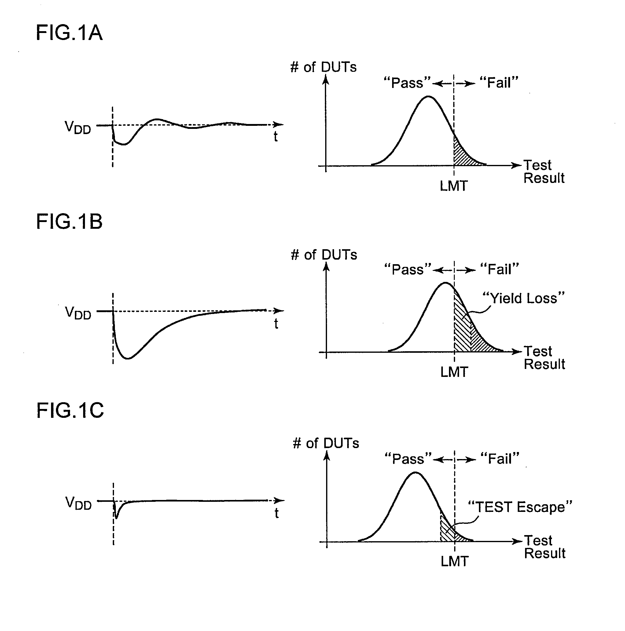
[0090]Description has been made in the embodiment regarding an arrangement in which the lower limit value of the power supply voltage is employed as the first characteristic value and the second characteristic value. However, the present invention is not restricted to such an arrangement.

[0091]With the first modification, as the first characteristic value, the propagation delay τUSR of a predetermined path (e.g., the critical path) in the DUT 1 in the user environment is employed. Furthermore, as the second characteristic value, the lower limit value VDD,MIN—ATE of the power supply signal in the tester environment is employed.

[0092]The measurement method for the propagation delay τUSR is not restricted in particular. For example, the propagation delay may be measured according to the following procedure.

[0093]That is to say, the quality of the DUT 1 is judged for each operation frequency while sweeping the operation frequency of the DUT 1. With such a test, the u...

second modification

[Second Modification]

[0097]With the second modification, as the first device characteristic value and the second device characteristic value, the upper limit of the operation frequency that allows the DUT 1 to operate normally when a rated power supply signal is supplied to the DUT 1 is employed.

[0098]In this case, the spec value XSPEC is determined based on the rated operation frequency of the DUT 1. For example, in a case in which the DUT 1 is configured as a device guaranteed to operate at 1 GHz, the spec value XSPEC is determined to be 1 GHz.

[0099]FIG. 9 is a diagram showing the relation between the first device characteristic value fMAX—USR and the second device characteristic value fMAX—ATE according to the second modification. With the first device characteristic value fMAX—USR as x and with the second device characteristic value fMAX—ATE as y, when the relation y=f(x) holds true, the condition setting unit 40 sets the operation frequency of the DUT 1 to be used in the main t...

third modification

[Third Modification]

[0100]As the first device characteristic value, the lower limit value VDD,MIN—USR of the power supply signal that allows the DUT 1 to operate normally when the DUT 1 is operated at a rated operation frequency is employed. Furthermore, as the second device characteristic value, the upper limit value fMAX—ATE of the operation frequency that allows the DUT 1 to operate normally when a rated power supply signal is supplied to the DUT 1 is employed. The spec value XSPEC is determined based on the rated value of the power supply signal. With the first device characteristic value VDD,MIN—USR as x and with the second device characteristic value fMAX—ATE as y, when the relation y=f(x) holds true, the condition setting unit 40 sets the operation frequency, at which the DUT 1 is operated in the main test, to yATE=f(XSPEC).

[0101]Such a modification also reduces divergence in the test results.


PUM


Abstract

A judgment unit judges the pass / fail of DUTs. A power supply circuit has changeable characteristics, and supplies a power supply signal to the DUTs. A condition setting unit performs a pilot test before a main test for the DUTs, and acquires a test condition to be used in the main test. The condition setting unit executes: (a) measuring a first device characteristic value for each of multiple pilot samples sampled from among the DUTs while emulating a power supply characteristic close to what is used in a user environment in which the DUT is actually used; (b) measuring a predetermined second device characteristic value for each of the multiple pilot sample devices while emulating a power supply characteristic close to what is used in a tester environment in which the main test is performed; and (c) determining the test condition based on the first and second device characteristic values.

Description

BACKGROUND OF THE INVENTION[0001]1. Field of the Invention[0002]The present invention relates to a test apparatus configured to test a device under test.[0003]2. Description of the Related Art[0004]In a testing operation for a semiconductor integrated circuit (which will be referred to as the “DUT” hereafter) that employs CMOS (Complementary Metal Oxide Semiconductor) technology such as a CPU (Central Processing Unit), DSP (Digital Signal Processor), memory, or the like, electrical current flows in a flip-flop or a latch included in the DUT while it operates receiving the supply of a clock. When the clock is stopped, the circuit enters a static state in which the amount of current decreases. Accordingly, the sum total of the operating current (load current) of the DUT changes over time depending on the content of the test operation, and so forth. Also, various kinds of analog circuits and various kinds of analog / digital hybrid circuits also have a problem of such a fluctuation in th...

Claims


Application Information

Patent Timeline
Patent Type & Authority Applications(United States)
IPC IPC(8): G01R31/28
CPCG01R31/2851G11C29/56008G01R31/31721G01R31/26H01L22/00
Inventor ISHIDA, MASAHIROKOMATSU, SATOSHIASADA, KUNIHIRONAKURA, TORU
Owner THE UNIV OF TOKYO
Why Eureka
Try Eureka