Resistive memory device and memory apparatus and data processing system having the same

a technology of resistive memory and memory apparatus, which is applied in the direction of digital storage, semiconductor devices, instruments, etc., can solve the problems of high power consumption, physical and electrical limitations of flash memory devices,

Inactive Publication Date: 2014-04-10
SK HYNIX INC
View PDF0 Cites 13 Cited by
  • Summary
  • Abstract
  • Description
  • Claims
  • Application Information

AI Technical Summary

Benefits of technology

[0024]According to one aspect of an exemplary embodiment, there is provided a resistive memory device. The resistive memory device may include: a first electrode layer; a second electrode layer; and a first variable resistive layer and a second variable resistive layer repeatedly stacked at least once between the first electrode layer and the second electrode layer. The first variable resistive material layer may include a metal nitride layer having a resistivity higher than that of the first electrode layer or the second electrode layer and less than or equal to that of an insulating material.

Problems solved by technology

Since flash memory devices operate at a low voltage for low power consumption, flash memory devices encounter physical and electrical limitations due to an insufficient current margin.
However, typical transition metal oxide results in high power consumption due to high driving voltage and current.
Sneak current, which flows in a path other than a selected device, occurs due to the high operation voltage and current.

Method used


Image

  • Resistive memory device and memory apparatus and data processing system having the same
  • Resistive memory device and memory apparatus and data processing system having the same
  • Resistive memory device and memory apparatus and data processing system having the same

Examples


Embodiment Construction

”.

BRIEF DESCRIPTION OF THE DRAWINGS

[0029]The above and other aspects, features and other advantages of the subject matter of the present disclosure will be more clearly understood from the following detailed description taken in conjunction with the accompanying drawings, in which:

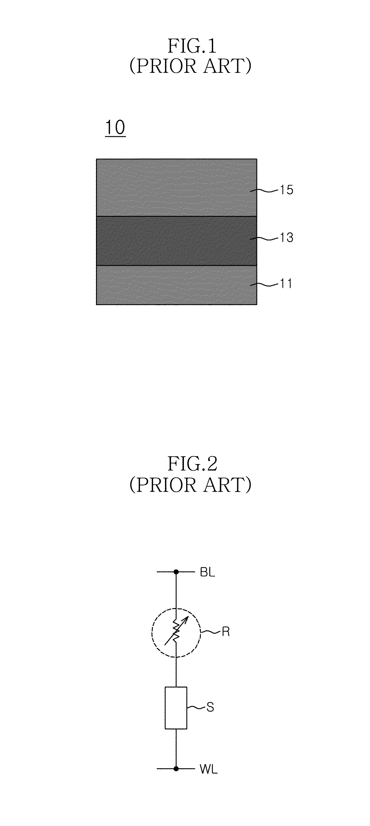
[0030]FIG. 1 illustrates a general resistive memory device;

[0031]FIG. 2 is a view illustrating a structure of a general resistive memory apparatus;

[0032]FIG. 3 is a graph illustrating a current / voltage characteristic of the resistive memory device of FIG. 1;

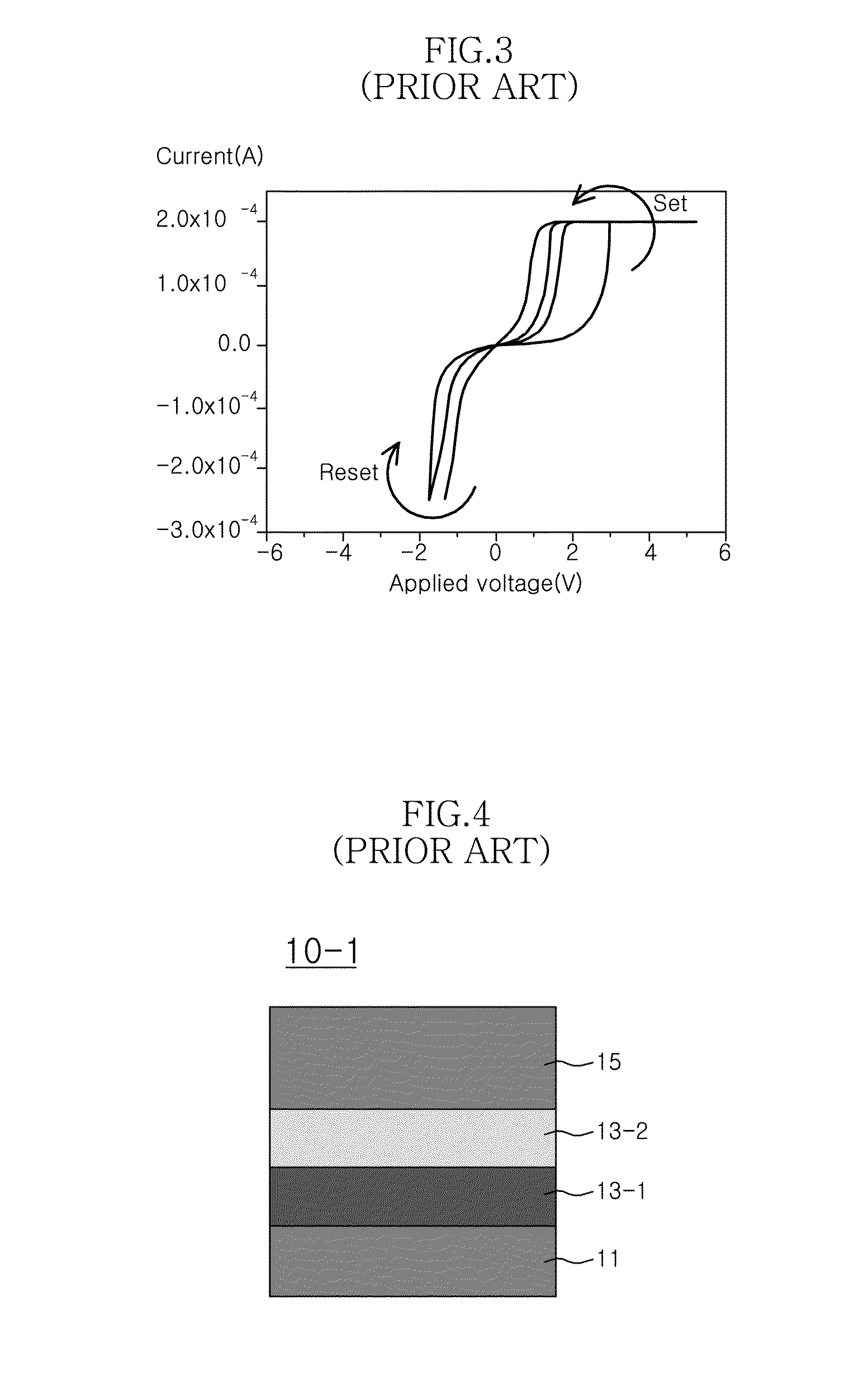
[0033]FIG. 4 illustrates another general resistive memory device;

[0034]FIG. 5 is a graph illustrating a current / voltage characteristic of the resistive memory device of FIG. 4;

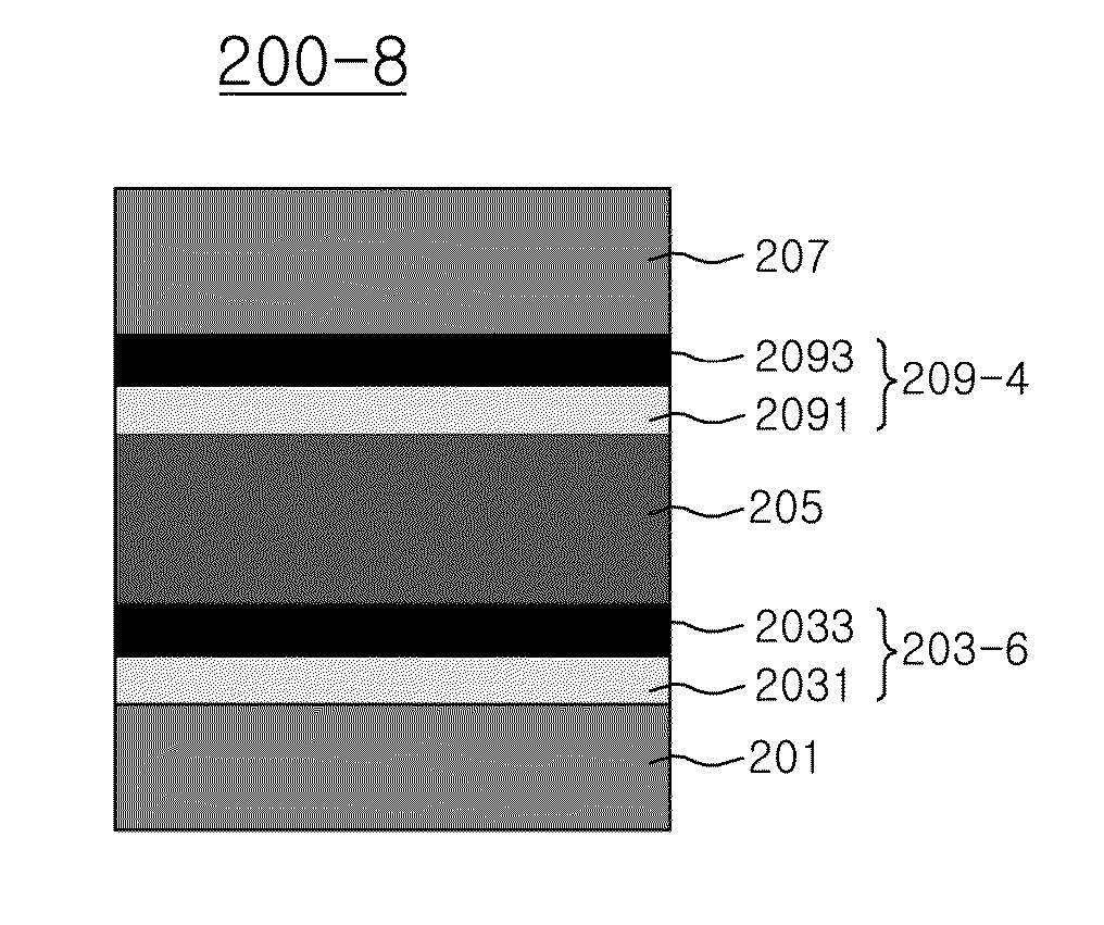
[0035]FIG. 6 is a view illustrating a structure of a resistive memory device according to an exemplary embodiment of the present invention;

[0036]FIG. 7 is a view illustrating a resistivity of an electrode layer and a second variable resistive material layer included in the resisti...


PUM


Abstract

A resistive memory device includes a first electrode layer, a second electrode layer, and a first variable resistive layer and a second variable resistive layer stacked at least once between the first electrode layer and the second electrode layer. The first variable resistive material layer may include a metal nitride layer having a resistivity higher than that of the first electrode layer or the second electrode layer and less than or equal to that of an insulating material.

Description

CROSS-REFERENCES TO RELATED APPLICATION[0001]This application claims priority under 35 U.S.C. 119(a) to Korean application number 10-2012-0111184, filed on Oct. 8, 2012, in the Korean Patent Office, which is incorporated by reference in its entirety.BACKGROUND OF THE INVENTION[0002]1. Technical Field[0003]The present invention relates to a semiconductor integrated device, and more particularly, to a resistive memory device and a memory apparatus, and a data processing system including the same.[0004]2. Related Art[0005]Flash memory devices which are representative of non-volatile memory devices have become increasingly more highly integrated. Recently, there is a need for a high integration technology below 20 nm. Since flash memory devices operate at a low voltage for low power consumption, flash memory devices encounter physical and electrical limitations due to an insufficient current margin. Thus, studies on non-volatile memory devices that can replace such flash memory devices ...

Claims


Application Information

Patent Timeline
Patent Type & Authority Applications(United States)
IPC IPC(8): H01L45/00
CPCH01L45/145H10N70/20H10N70/883H10N70/023H10N70/8833H10N70/826G11C11/15
Inventor PARK, WOO YOUNGLEE, KEE JEUNGKIM, BEOM YONG
Owner SK HYNIX INC
Why Eureka
Try Eureka