Electronic Device for Protection against Electrostatic Discharges, with a Concentric Structure

a concentric structure and electrostatic discharge technology, applied in the direction of semiconductor devices, diodes, electrical devices, etc., can solve the problems of silicon surface area occupation and other problems, and achieve the effect of reducing parasitic capacitance, reducing surface area, and reducing the integrity of input/output signals

Active Publication Date: 2014-04-10
STMICROELECTRONICS SRL
View PDF13 Cites 3 Cited by
  • Summary
  • Abstract
  • Description
  • Claims
  • Application Information

AI Technical Summary

Benefits of technology

[0007]The protection device is therefore intended to absorb this current pulse and prevent excess voltages across the terminals of the module.
[0011]In one embodiment, an integrated electronic component is proposed, for use in an ESD protection device in particular, this component having a completely novel topology, making its construction highly compact, and being scalable, while also being capable of absorbing large ESD pulses.
[0012]In particular, this results in a reduction of the surface area and a reduction of the parasitic capacitances.
[0015]Thus, in one embodiment, the component incorporates, in topological terms, R(M−1) triac structures, and the number of triac structures can be changed by changing R and M. The component is therefore easily scalable.
[0018]Thus these embodiments offer increased scalability for the component. This is because annular electrodes can be interconnected in a number of ways, making it possible to choose the sectors of the component that are to dissipate the energy of an ESD pulse. It is therefore possible to produce components with higher or lower robustness to heat dissipation.
[0021]In a variant, the component can comprise electrical contact areas on each of the annular semiconductor layers. This enables the gate current to be distributed more efficiently for more efficient triggering of the component in the presence of an ESD pulse.

Problems solved by technology

The width of each diode is generally large, typically 150 microns, resulting in a considerable occupation of surface area on silicon.

Method used


Image

  • Electronic Device for Protection against Electrostatic Discharges, with a Concentric Structure
  • Electronic Device for Protection against Electrostatic Discharges, with a Concentric Structure
  • Electronic Device for Protection against Electrostatic Discharges, with a Concentric Structure

Examples


Embodiment Construction

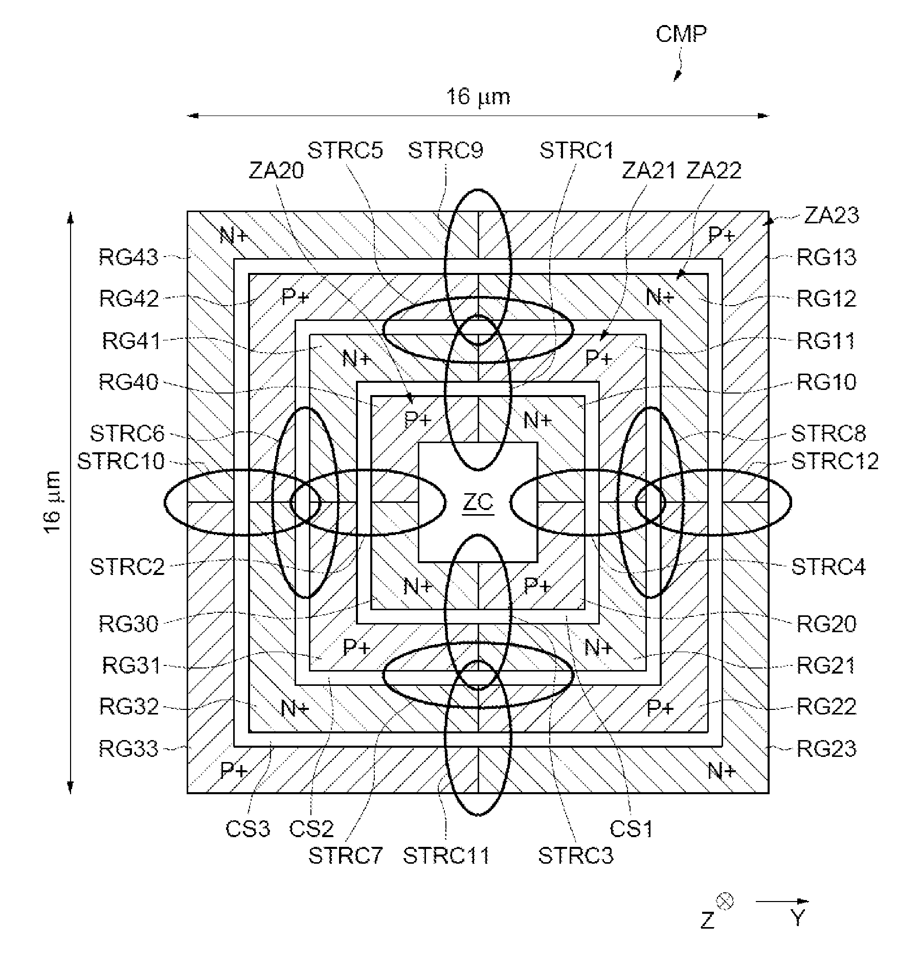
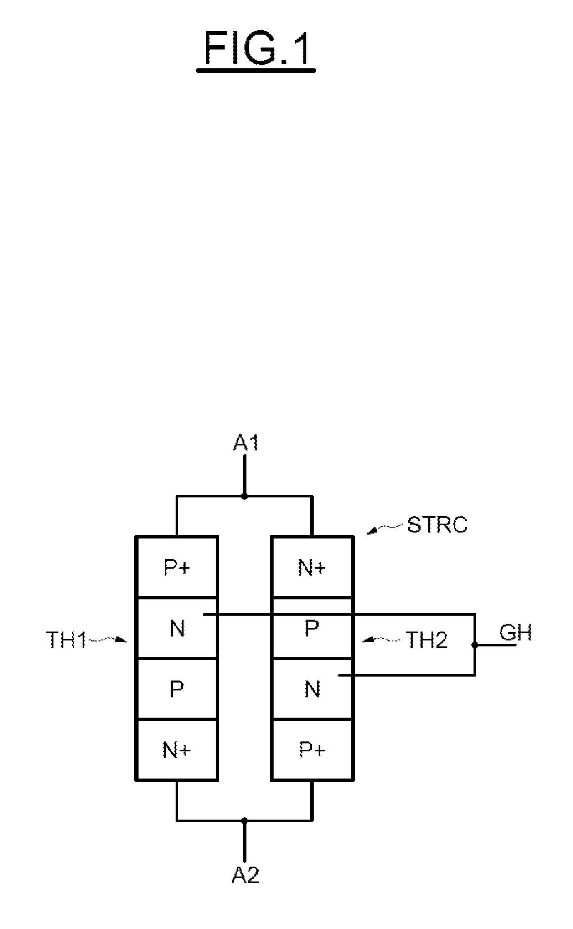
[0027]In FIG. 1, the reference STRC denotes a triac structure forming, as described below, an elementary member of one embodiment of an electronic component according to the invention.

[0028]This triac structure STRC includes two thyristors TH1, TH2. In this case, the thyristor TH1 includes four semiconductor zones having, respectively, p-, n-, p- and n-type conductivity, while the thyristor TH2 includes four semiconductor zones having, respectively, n-, p-, n- and p-type conductivity.

[0029]The p+ and n+ type end semiconductor zones of the two thyristors TH1, TH2 form the two electrodes A1, A2 of the triac structure STRC.

[0030]Additionally, the other two semiconductor zones, having n-type conductivity, of the two thyristors TH1 and TH2 form a single gate GH for the triac structure.

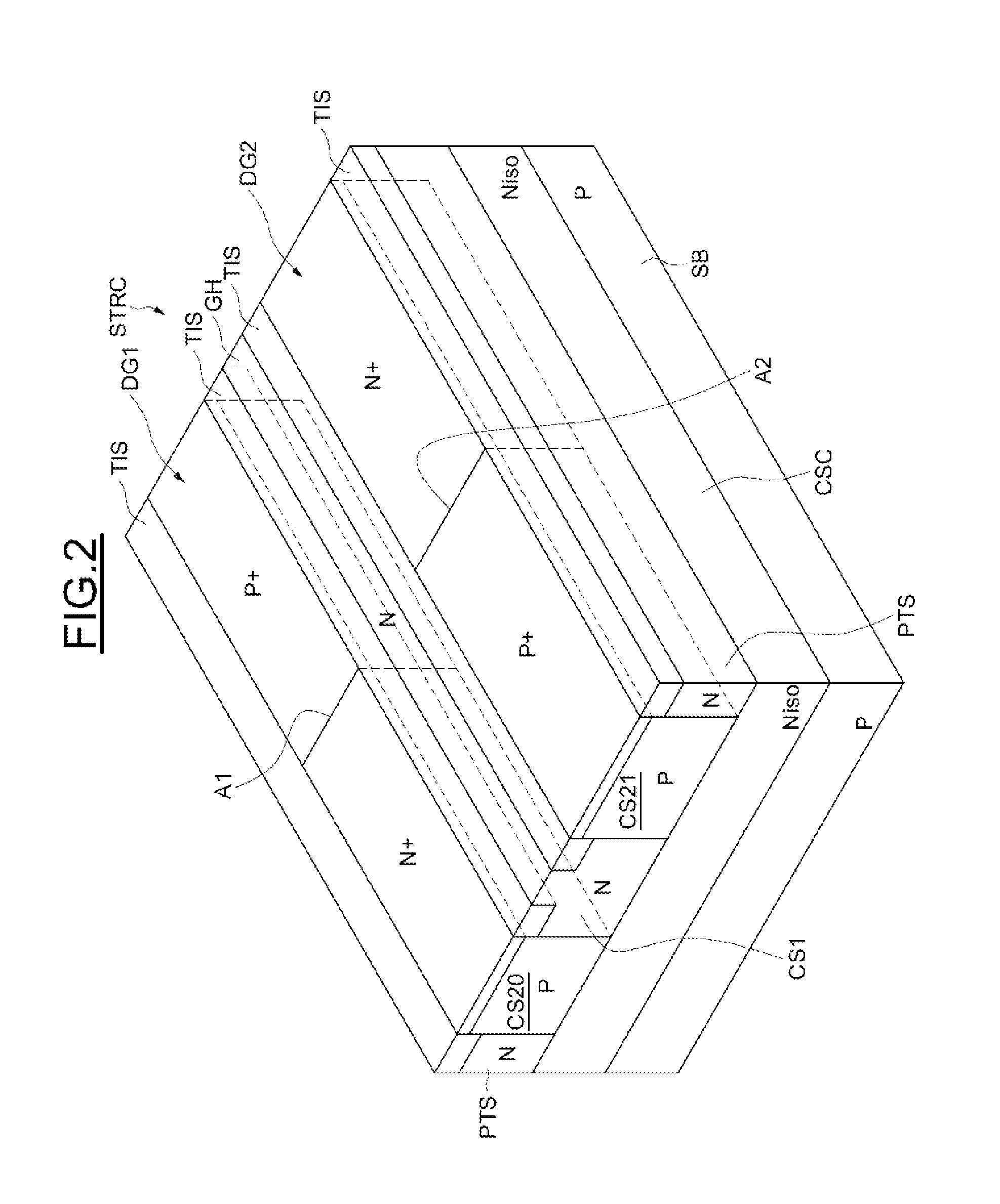
[0031]In topological terms, as shown in FIG. 2, the triac structure STRC includes, within a semiconductor substrate SB, having p-type conductivity for example, two semiconductor tanks CS20 and CS21, each ha...


PUM


Abstract

The component incorporates, in topological terms, a scalable number of triac structures in a concentric annular arrangement. The component can be used with an electronic device to protect against electrostatic discharges. For example, the components can be used to protect the input / output pad, the first power supply terminal, and the second power supply terminal of an integrated circuit against electrostatic discharges.

Description

[0001]This application claims priority to French Patent Application No. 1252194, which was filed Mar. 12, 2012 and is incorporated herein by reference.TECHNICAL FIELD[0002]The invention relates to integrated electronic components, and notably to those intended for the protection of nodes against electrostatic discharges (ESD).BACKGROUND[0003]An electronic module to be protected is connected between two power supply nodes and also, in some cases, to an input / output node intended to receive and deliver an input / output signal. For instance, when the module is in operation, one of the power supply nodes can be connected to a positive voltage and the other node can be connected to a negative or zero voltage (ground).[0004]When the module is not operational, it may be subjected to an electrostatic discharge typically taking the form of a very brief current pulse (with a typical duration of several microseconds) between two of the nodes, with a maximum current of about 2 amperes, for examp...

Claims


Application Information

Patent Timeline
Patent Type & Authority Applications(United States)
IPC IPC(8): H01L27/02
CPCH01L27/0259H01L29/7436H01L29/747H01L27/0262H01L29/87
Inventor JIMENEZ, JEANGALY, PHILIPPEHEITZ, BORIS
Owner STMICROELECTRONICS SRL
Why Eureka
Try Eureka