Method for using sputtering target and method for manufacturing oxide film

a technology of sputtering target and oxide film, which is applied in the direction of polycrystalline material growth, crystal growth process, vacuum evaporation coating, etc., can solve the problems of unstable properties, difficult to secure transistor reliability, and high cost, and achieve favorable transistor characteristics and high long-term reliability.

Inactive Publication Date: 2014-04-17
SEMICON ENERGY LAB CO LTD
View PDF6 Cites 57 Cited by
  • Summary
  • Abstract
  • Description
  • Claims
  • Application Information

AI Technical Summary

Benefits of technology

[0019]In the case where an oxide film containing a metal element as described above is used for a channel formation region of a transistor, it is required for the oxide film to enable the transistor to exhibit favorable transistor characteristics and have high long-term reliability.

Problems solved by technology

Although the oxide film containing a metal element has high controllability of the carrier density and can provide transistor characteristics with relative ease, it has the problem of being likely to become amorphous and having unstable properties.
Therefore, it has been difficult to secure transistor reliability.

Method used


Image

  • Method for using sputtering target and method for manufacturing oxide film
  • Method for using sputtering target and method for manufacturing oxide film
  • Method for using sputtering target and method for manufacturing oxide film

Examples


first embodiment

1. First Embodiment

Sputtering Method and Mechanism Thereof

[0096]In this embodiment, a method for forming a film by sputtering in one embodiment of the present invention and a mechanism thereof will be described.

[1.1. Film Formation Conditions or Environment]

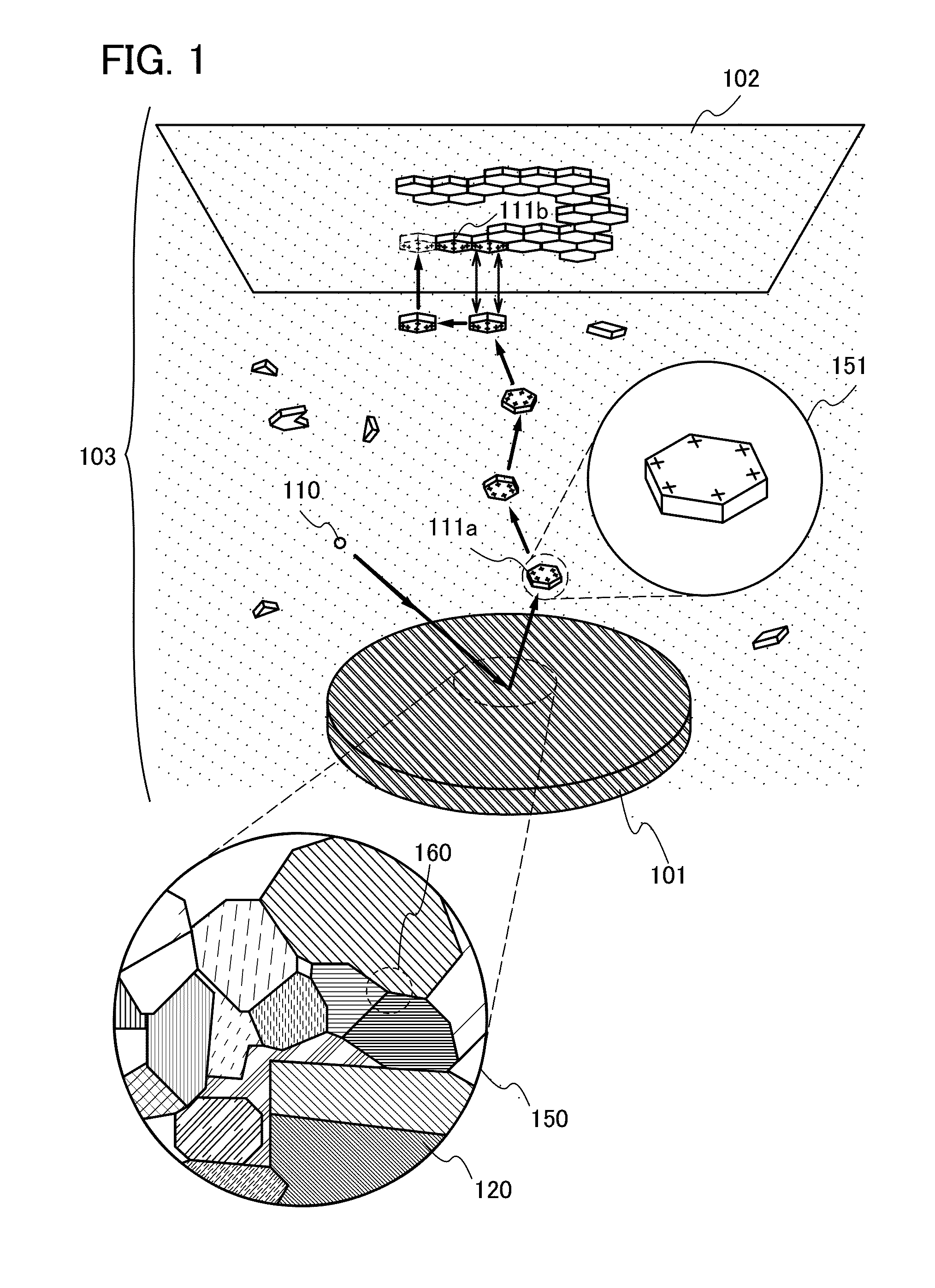
[0097]FIG. 1 is a schematic diagram illustrating how an oxide film is formed on a deposition surface 102 using a sputtering target 101.

[0098]First, the sputtering target 101 illustrated in FIG. 1 and used for the formation of the oxide film will be described.

[0099]As illustrated in an enlarged portion 150 of part of the sputtering target 101, the sputtering target 101 contains a polycrystalline oxide including a plurality of crystal grains 120. For the sputtering target 101, a compound containing indium (In), gallium (Ga), zinc (Zn), and oxygen (O) can be used as a material, for example.

[0100]Although the sputtering target 101 in FIG. 1 has a circular shape, the shape is not limited to the circular shape and may be a rectangular ...

second embodiment

2. Second Embodiment

Sputtering Target

[0137]In this embodiment, a sputtering target in one embodiment of the present invention will be described with reference to FIGS. 3A and 3B and FIG. 4.

[2.1. Sputtering Target]

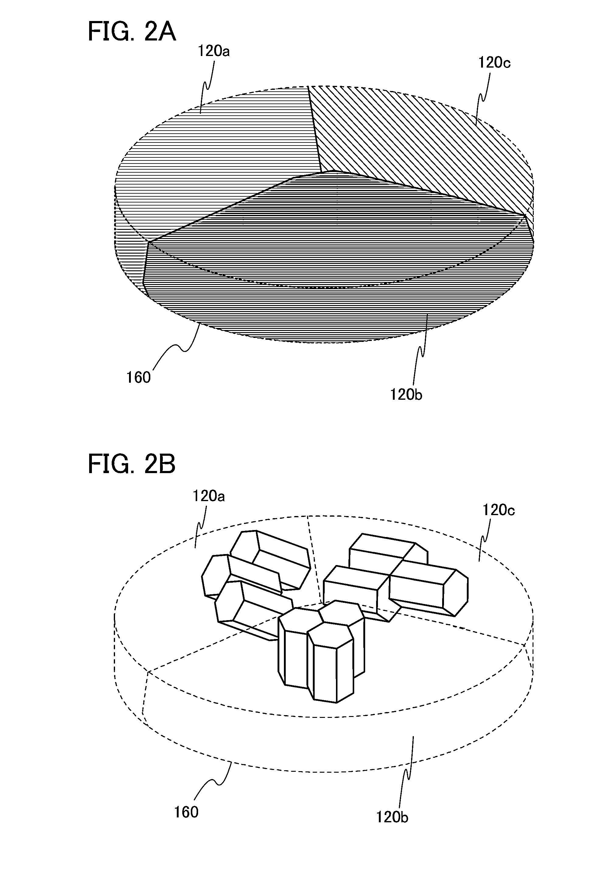
[0138]A sputtering target in one embodiment of the present invention contains a polycrystalline oxide including a plurality of crystal grains with randomly oriented c-axes.

[0139]The plurality of crystal grains included in the sputtering target have a cleavage plane. The cleavage plane is, for example, a plane parallel to the a-b planes.

[0140]In the case where the plurality of crystal grains included in the sputtering target have a hexagonal crystal structure, a flat-plate-like sputtered particle separated in sputtering has a crystal structure in the form of a hexagonal prism having substantially regular hexagonal upper and lower surfaces with an interior angle of 120°.

[0141]The sputtered particle is ideally single crystal, but may be partly amorphous due to the effect of co...

third embodiment

3. Third Embodiment

Film Formation Apparatus

[0181]In this embodiment, a film formation apparatus in one embodiment of the present invention will be described with reference to FIG. 6, FIGS. 7A and 7B, FIGS. 8A and 8B, and FIG. 9.

[0182]Note that the film formation apparatus described below includes at least a film formation chamber (a sputtering chamber) where film formation is performed by a sputtering method. The sputtering method here is classified according to the method for generating plasma. A sputtering method using a direct-current (DC) power source is referred to as a direct-current sputtering method; a sputtering method using an alternate-current (AC) power source is referred to as an alternate-current sputtering method; and a sputtering method using a high-frequency (RF) power source is referred to as a high-frequency sputtering method. Among these methods, the direct-current sputtering method is industrially superior in terms of productivity and manufacturing cost because ...


PUM

PropertyMeasurementUnit
temperatureaaaaaaaaaa
angleaaaaaaaaaa

Abstract

A plasma space containing an ionized inert gas is formed in contact with a deposition surface and a surface of a sputtering target containing a polycrystalline oxide including a plurality of crystal grains with randomly oriented c-axes. A flat-plate-like sputtered particle is separated from a cleavage plane corresponding to a-b planes of the plurality of crystal grains by collision of the ionized inert gas with the surface of the sputtering target. The flat-plate-like sputtered particle is transferred to the deposition surface through the plasma space with its flat-plate-like shape substantially maintained. The flat-plate-like sputtered particle and another flat-plate-like sputtered particle charged with the same polarity repel each other and are deposited on the deposition surface so as to be adjacent to each other on a plane such that the c-axes are substantially perpendicular to the deposition surface.

Description

BACKGROUND OF THE INVENTION[0001]1. Field of the Invention[0002]The present invention relates to a sputtering target, a method for manufacturing a sputtering target, a method for using a sputtering target, a sputtering apparatus, a method for using a sputtering apparatus, an oxide film, a method for manufacturing an oxide film, a semiconductor device manufactured using an oxide film, and an electric device including a semiconductor device manufactured using an oxide film.[0003]2. Description of the Related Art[0004]Semiconductor elements, e.g., transistors manufactured using a semiconductor thin film which is formed over a substrate having an insulating surface such as a glass substrate (such transistors are also referred to as thin film transistors or TFTs for short) and diodes, are applied to a wide range of semiconductor devices such as integrated circuits (ICs) and image display devices (simply also referred to as display devices). A silicon-based semiconductor material is widel...

Claims


Application Information

Patent Timeline
Patent Type & Authority Applications(United States)
IPC IPC(8): C23C14/34
CPCC23C14/34C23C14/08C23C14/3414C23C14/564C30B23/00C30B23/005C30B29/22H01L21/02554H01L21/02565H01L21/02631H01L21/28194H01L29/51H01L29/513H01L29/66969H01L29/7869H01L27/1225
Inventor YAMAZAKI, SHUNPEI
Owner SEMICON ENERGY LAB CO LTD
Why Eureka
Try Eureka