Light-emitting device

a technology of light-emitting devices and light-emitting tubes, which is applied in the direction of semiconductor devices, basic electric elements, electrical equipment, etc., can solve the problems of crosstalk phenomenon, large current flow, and deterioration of organic el elements

Active Publication Date: 2014-04-17
SEMICON ENERGY LAB CO LTD +1
View PDF9 Cites 29 Cited by
  • Summary
  • Abstract
  • Description
  • Claims
  • Application Information

AI Technical Summary

Benefits of technology

[0029]In accordance with one embodiment of the present invention, occurrence of a cross

Problems solved by technology

However, a large current flow accelerates deterioration of organic EL elements.
One problem of a light-e

Method used


Image

  • Light-emitting device
  • Light-emitting device
  • Light-emitting device

Examples


embodiment 1

Structure of Display Panel

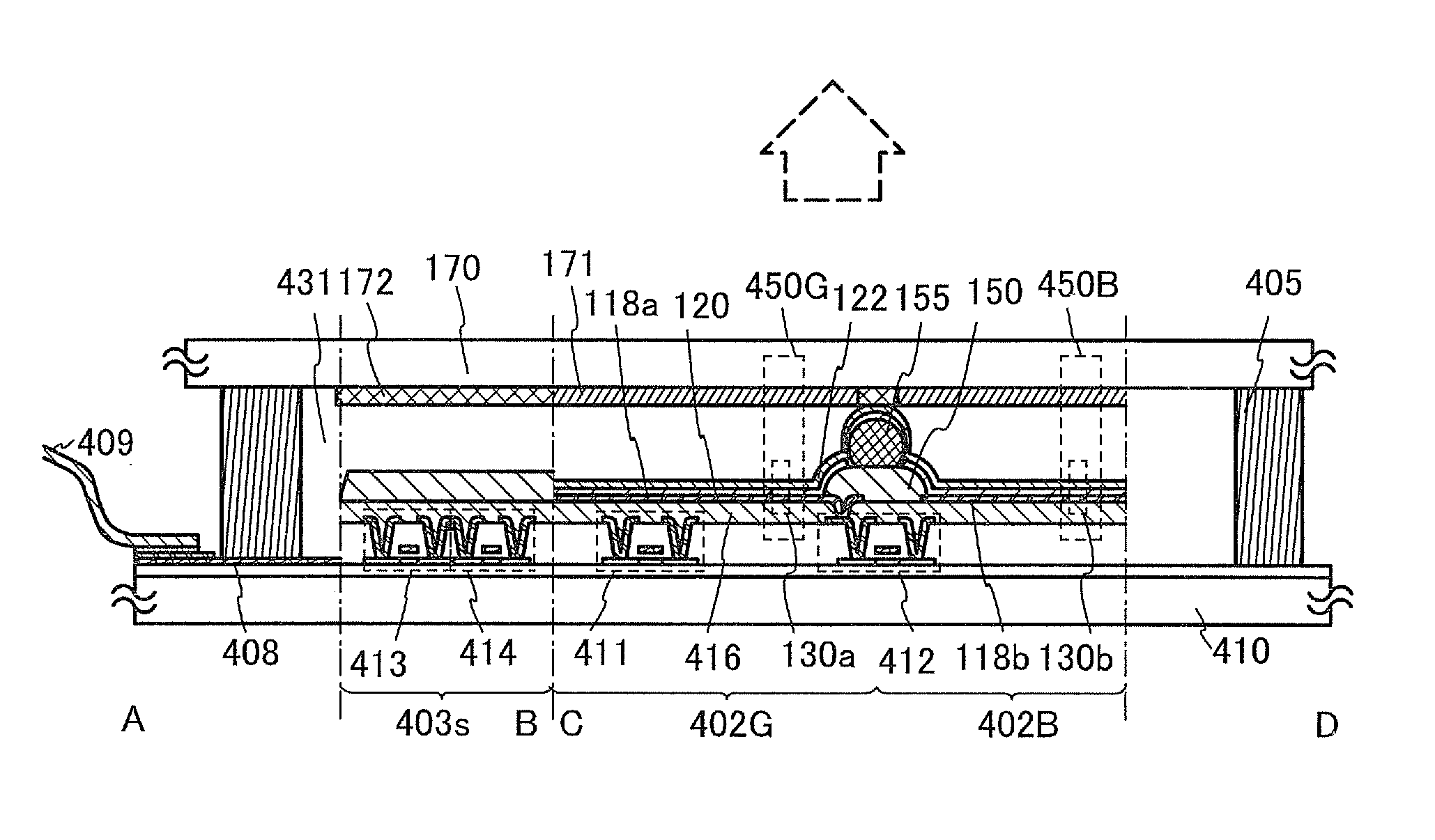
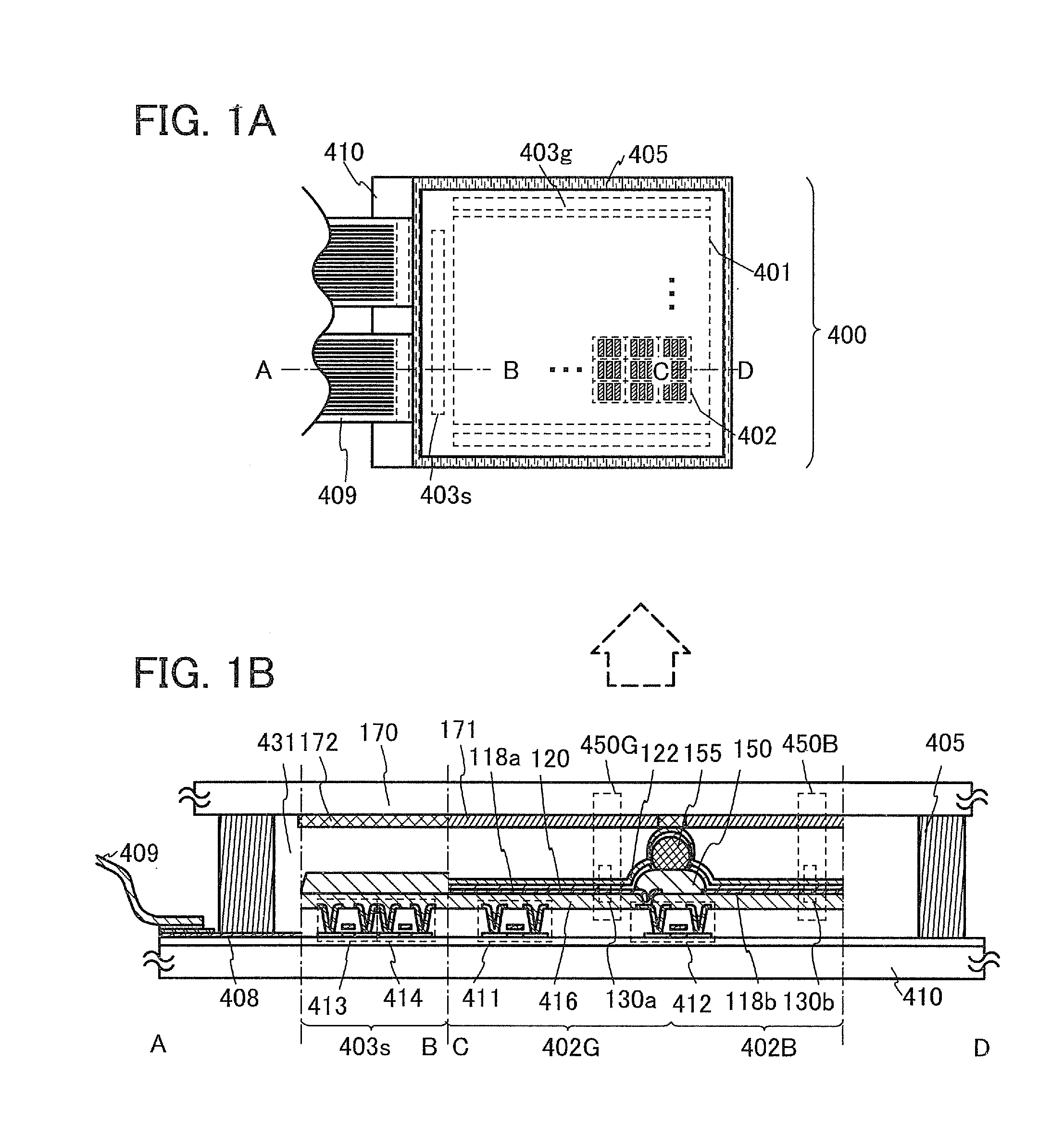
[0044]FIGS. 1A and 1B illustrate a structure of a display panel which can be used for a display device in one embodiment of the present invention. FIG. 1A is a top view of the structure of the display panel which can be used for a display device in one embodiment of the present invention, and FIG. 1B is a side view of the structure including cross sections along section lines A-B and C-D in FIG. 1A.

[0045]A display panel 400 shown as an example in this embodiment includes a display portion 401 over a first substrate 410. The display portion 401 includes a plurality of pixels 402. The pixel 402 includes a plurality of sub-pixels (e.g., three sub-pixels) (see FIG. 1A). Over the first substrate 410, in addition to the display portion 401, a source side driver circuit portion 403s and a gate side driver circuit portion 403g which drive the display portion 401 are provided. Note that the driver circuit portions can be provided not over the first substrate 410 but...

embodiment 2

[0106]A configuration example of a light-emitting element which can be used in a light-emitting module of one embodiment of the present invention is described with reference to FIGS. 5A to 5C.

[0107]The light-emitting element shown as an example in this embodiment includes a lower electrode, an upper electrode, and an organic layer between the lower electrode and the upper electrode. One of the lower and upper electrodes functions as an anode, and the other functions as a cathode. The organic layer is provided between the lower electrode and the upper electrode, and a structure of the organic layer may be appropriately determined in accordance with materials of the lower electrode and the upper electrode.

Configuration Example of Light-Emitting Element

[0108]An example of a configuration of the light-emitting element is illustrated in FIG. 5A. In the light-emitting element illustrated in FIG. 5A, an organic layer including a light-emitting unit 1103a and a light-emitting unit 1103b is ...

example

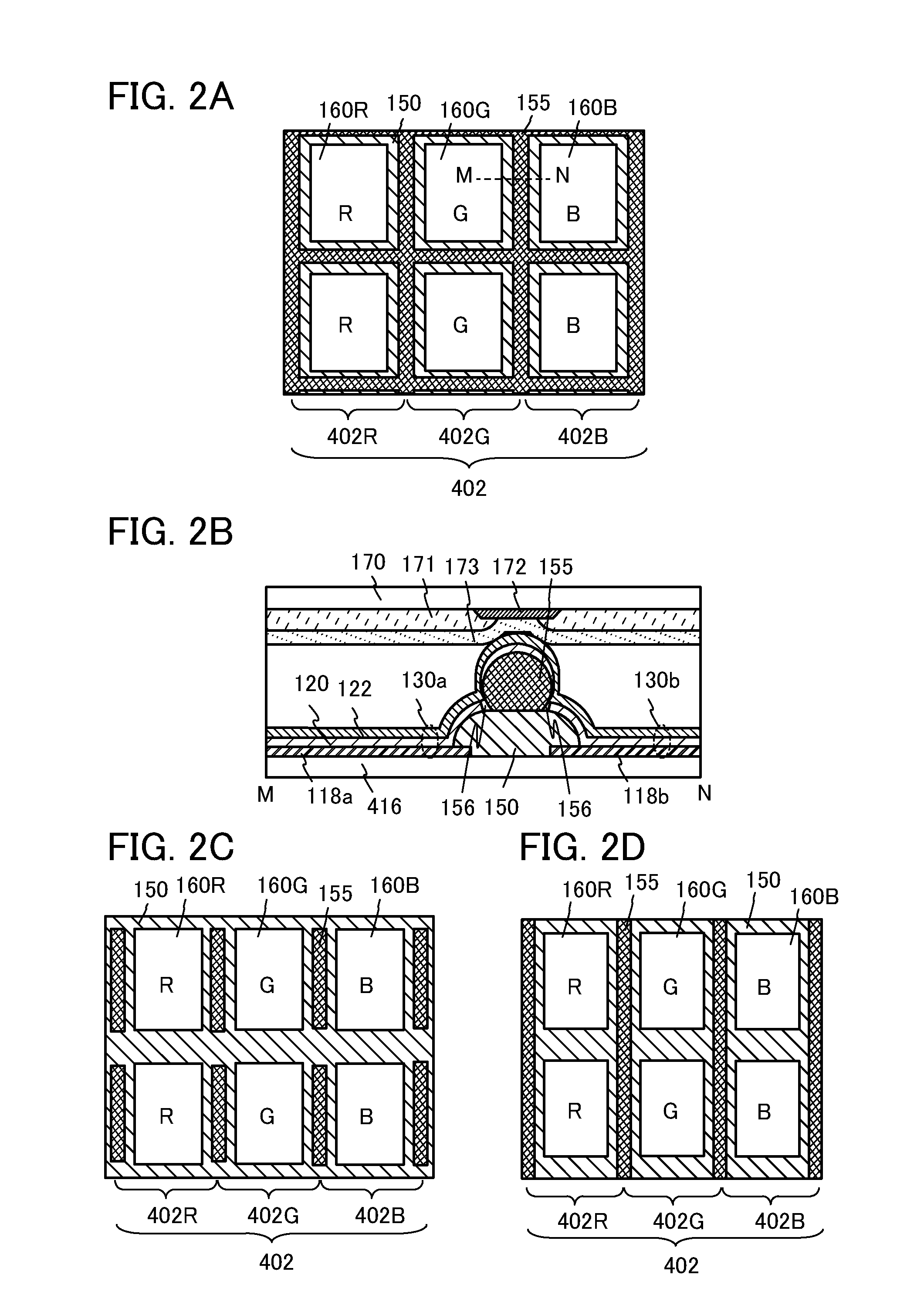
[0149]FIG. 7A is a photograph showing the cross-sectional structure of a partition and a spacer (projecting object) of a light-emitting element of Example. FIG. 7B is an enlarged photograph showing the recess 153 formed by a side surface of the spacer and a side surface of the partition which is shown in FIG. 7A. FIG. 7C is an enlarged photograph showing the region 154 shown in FIG. 7A.

[0150]The position of the spacer 155 in this example is similar to that in FIG. 4B, and the end portion of the spacer 155 is laid out over the inclined portion of the surface of the partition 150.

[0151]The materials included in the light-emitting element of this example are given below.

[0152]The first lower electrode 118a and the second lower electrode 118b: a stack of an aluminum-nickel alloy film containing lanthanum (thickness: 200 nm) and a titanium film (thickness: 6 nm)

[0153]A microcavity structure 149: an indium tin oxide film containing silicon oxide (ITSO) (thicknesses: 0 nm in a light-emitti...


PUM


Abstract

Occurrence of a crosstalk phenomenon is suppressed in a light-emitting device including a tandem element. A light-emitting device includes a first lower electrode and a second lower electrode over an insulating layer; a partition which is formed over the insulating layer and positioned between the first lower electrode and the second lower electrode; a projecting object formed over the partition; a first light-emitting unit over each of the first lower electrode, the partition, the projecting object, and the second lower electrode; an intermediate layer over the first light-emitting unit; a second light-emitting unit over the intermediate layer; and an upper electrode over the second light-emitting unit. A recess is formed by a side surface of the projecting object and a side surface of the partition.

Description

BACKGROUND OF THE INVENTION[0001]1. Field of the Invention[0002]One embodiment of the present invention relates to a light-emitting device including a tandem element.[0003]2. Description of the Related Art[0004]Commercialization of organic EL displays is accelerating. Displays are increasingly required to provide high luminance for outdoor use. It is known that the luminance of an organic EL element increases in proportion to electric current and light emission at high luminance can be achieved.[0005]However, a large current flow accelerates deterioration of organic EL elements. Thus, if high luminance can be achieved with a small amount of current, light-emitting elements can have longer lifetime. In this regard, a tandem element in which a plurality of light-emitting units is stacked has been proposed as a light-emitting element capable of providing high luminance with a small amount of current (see Patent Document 1, for example).[0006]Note that in this specification, a light-emi...

Claims


Application Information

Patent Timeline
IPC IPC(8): H01L33/36
CPCH01L33/36H10K59/32H10K59/122H10K50/131H10K50/8428
Inventor HATANO, KAORUSENDA, NAOYUKINIBOSHI, MANABUKIKUCHI, KATSUHIROKAWATO, SHINICHIOCHI, TAKASHITSUKAMOTO, YUTOKOSAKA, TOMOHIROOSAKI, TOMOFUMI
Owner SEMICON ENERGY LAB CO LTD
Why Eureka
Try Eureka