Liquid crystal display device and touch panel

Active Publication Date: 2014-04-17
SEMICON ENERGY LAB CO LTD
View PDF10 Cites 14 Cited by
  • Summary
  • Abstract
  • Description
  • Claims
  • Application Information

AI Technical Summary

Benefits of technology

[0025]According to the technique disclosed in this specification, a liquid crystal display device having as h

Problems solved by technology

For that reason, a liquid crystal display device is manufactured using a material containing water as little as possible and by a structure and a manufacturing method which prevents entry of water as much as possible, which leads to resolution of decrease in reliability.
However, limitation of a material causes new problems in that display quality of a liquid crystal display device is decreased

Method used


Image

  • Liquid crystal display device and touch panel
  • Liquid crystal display device and touch panel
  • Liquid crystal display device and touch panel

Examples


embodiment 1

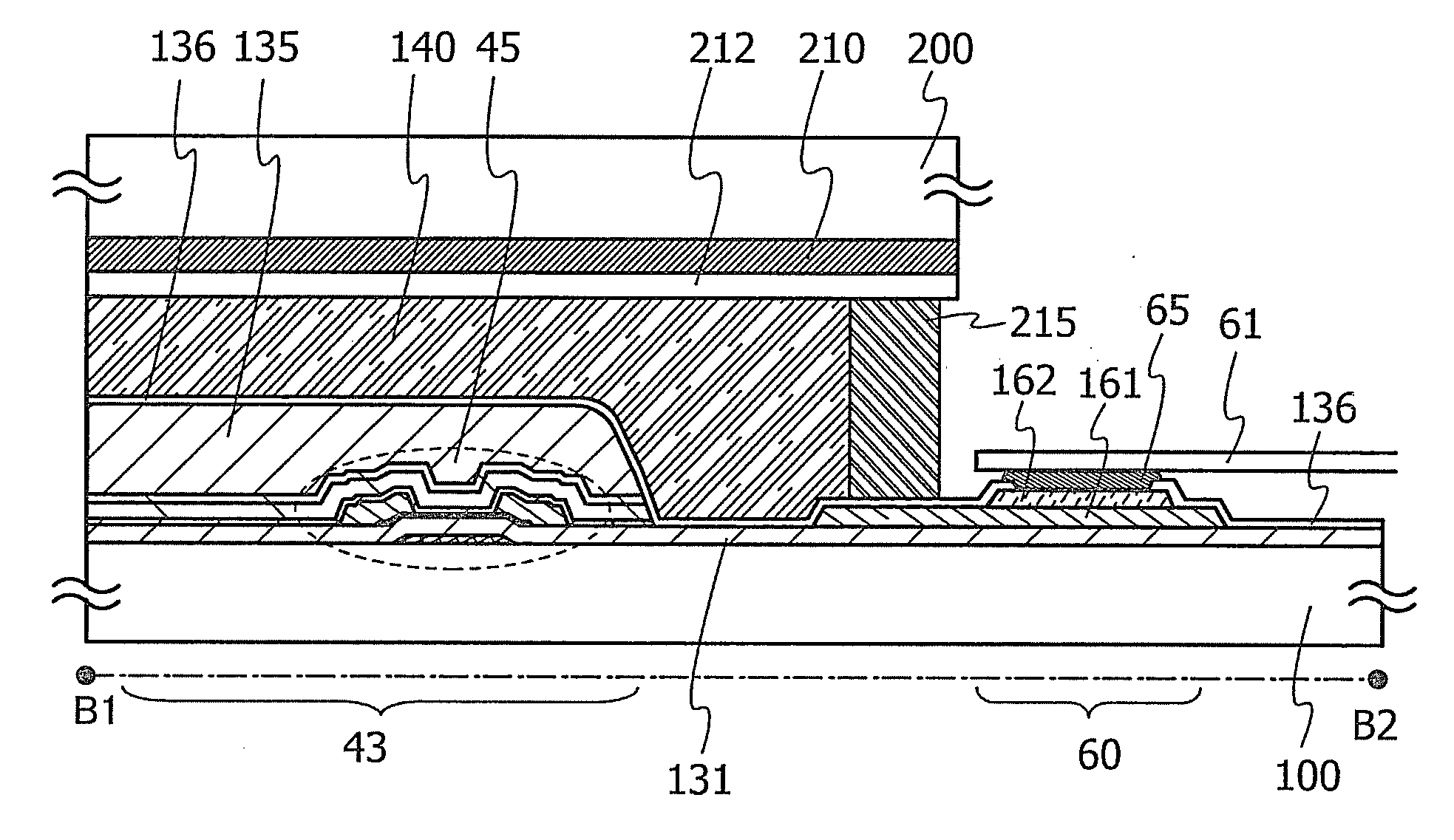
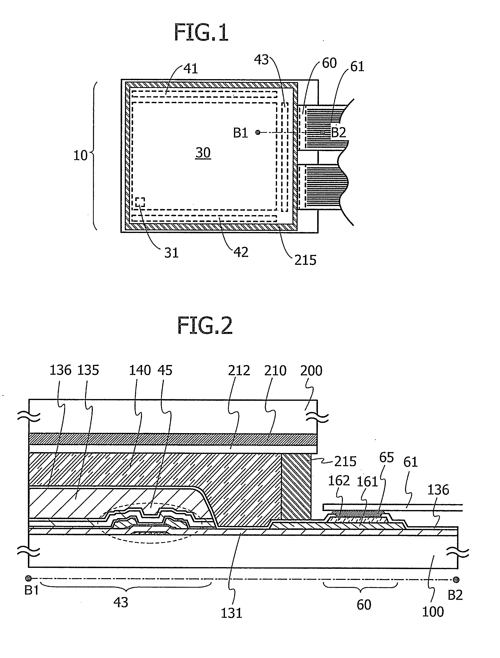
[0054]A liquid crystal panel of one embodiment of the present invention is described with reference to FIG. 1 to FIG. 6 and FIGS. 10A and 10B.

[0055]FIG. 10A is a block diagram illustrating a structural example of a liquid crystal panel 10. The liquid crystal panel 10 includes a display portion 30, a scan line driver circuit 41, a scan line driver circuit 42, and a data line driver circuit 43. In the liquid crystal panel 10, the driver circuits 41 to 43 and the display portion 30 are formed over the same substrate, a board 100; thus, the liquid crystal panel 10 is also referred to as a liquid crystal module. The liquid crystal panel 10, a control circuit thereof, a power supply circuit, a back light module, and the like are incorporated in a housing, so that a liquid crystal display device is completed.

[0056]The display portion 30 includes a plurality of pixels 31 each of which is connected to a scan line 110 and a data line 111. FIG. 10B is a circuit diagram showing a structural exa...

embodiment 2

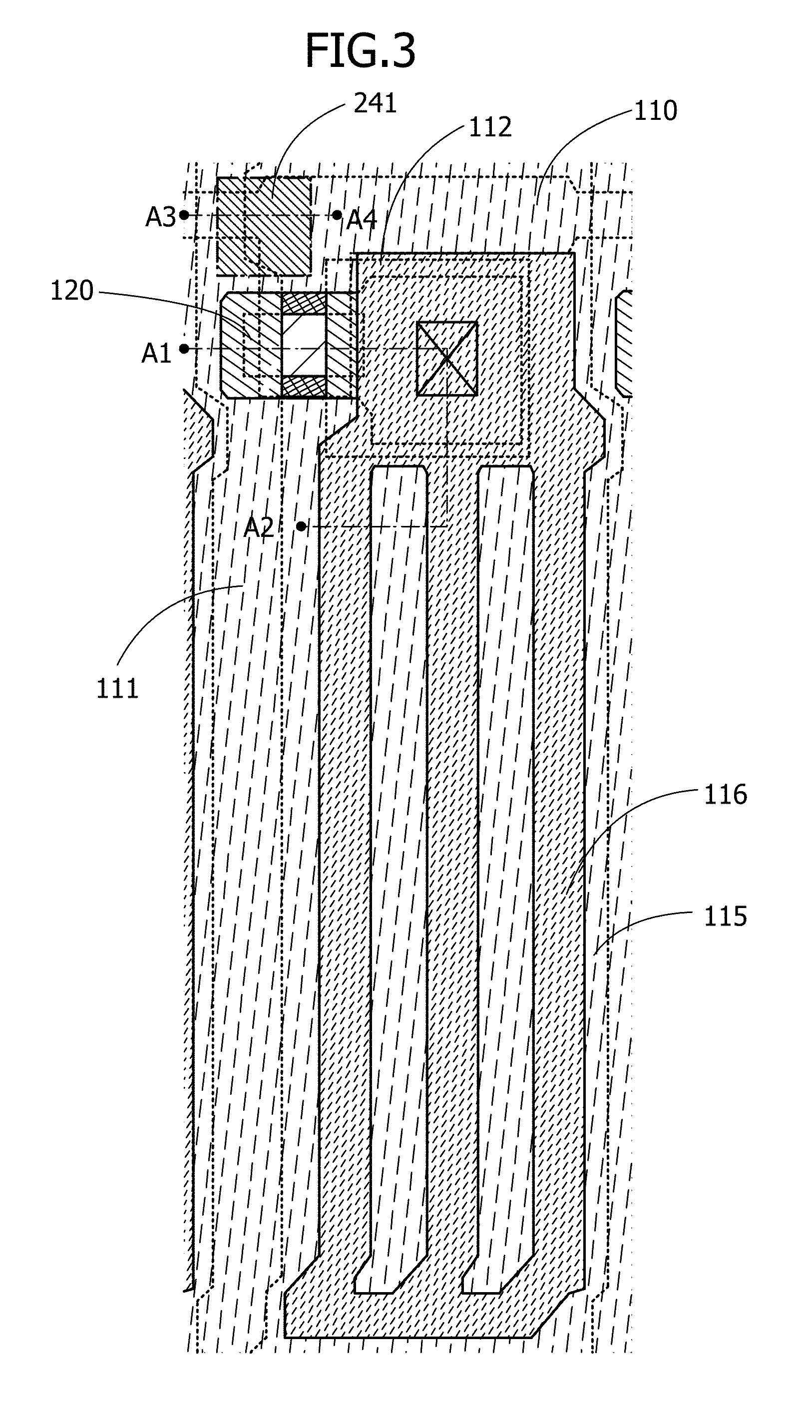
[0145]In this embodiment, a transistor included in the pixel 31 and the driver circuits 41 to 43 of the liquid crystal panel 10 is described.

120>

[0146]As the oxide semiconductor used for the semiconductor layer 120 of a transistor, for example, any of the following can be used: indium oxide, tin oxide, zinc oxide, an In—Zn-based oxide, a Sn—Zn-based oxide, an Al—Zn-based oxide, a Zn—Mg-based oxide, a Sn—Mg-based oxide, an In—Mg-based oxide, an In—Ga-based oxide, an In—Ga—Zn-based oxide (also referred to as IGZO), an In—Al—Zn-based oxide, an In—Sn—Zn-based oxide, a Sn—Ga—Zn-based oxide, an Al—Ga—Zn-based oxide, a Sn—Al—Zn-based oxide, an In—Hf—Zn-based oxide, an In—Zr—Zn-based oxide, an In—Ti—Zn-based oxide, an In—Sc—Zn-based oxide, an In—Y—Zn-based oxide, an In—La—Zn-based oxide, an In—Ce—Zn-based oxide, an In—Pr—Zn-based oxide, an In—Nd—Zn-based oxide, an In—Sm—Zn-based oxide, an In—Eu—Zn-based oxide, an In—Gd—Zn-based oxide, an In—Tb—Zn-based oxide, an In—Dy—Zn-based oxide, an In—...

embodiment 3

[0196]The liquid crystal panel 10 in FIG. 1 provided with a touch sensor (contact detector) can function as a touch panel.

[0197]In this embodiment, a touch panel is described with reference to FIG. 12, FIG. 13, and FIGS. 14A and 14B.

[0198]FIG. 12 is a cross-sectional view illustrating a structural example of a touch panel 400 using the liquid crystal panel 10. FIG. 13 is a plan view illustrating a structural example of the common electrode 421 and the electrode 422 of the touch panel 400. FIG. 14A is a cross-sectional view taken along line C1-C2 in FIG. 13, and FIG. 14B is a plan view of a region 240 in FIG. 13.

[0199]The touch panel 400 includes a capacitive sensor as a touch sensor. A polarizing plate 411 is attached to the outer side of the substrate 100, and a polarizing plate 412 is attached to the outer side of the substrate 200.

[0200]A common electrode 421 over the substrate 100 serves as a common electrode of a pixel and an electrode of a capacitor in the touch sensor. The el...


PUM


Abstract

A semiconductor layer of a transistor is formed of an oxide semiconductor film including a crystal part. An organic resin film covering the transistor is formed. By treatment such as drying treatment on the organic resin film in a cell process, variations in the threshold voltage of the oxide semiconductor transistor due to moisture can be suppressed. A common electrode faces a pixel electrode. The common electrode and the pixel electrode are formed over the organic resin film with an insulating film provided therebetween. Therefore, a capacitor can be provided to a liquid crystal element if a pixel does not include a wiring for a storage capacitor. An antistatic electrode is provided on the outer side of a color filter substrate and the capacitance between the antistatic electrode and the common electrode is utilized, so that the liquid crystal display device can be used as a touch panel.

Description

BACKGROUND OF THE INVENTION[0001]1. Field of the Invention[0002]The present invention relates to a liquid crystal display device including a transistor using an oxide semiconductor and a touch panel including the liquid crystal display device.[0003]2. Description of the Related Art[0004]Transistors which are used for many liquid crystal display devices and organic EL display devices have been formed using a silicon semiconductor film such as an amorphous silicon film or a polycrystalline silicon film.[0005]Instead of the silicon semiconductor film, a technique in which an oxide semiconductor film is used for transistors has attracted attention.[0006]For example, a technique is disclosed in which a transistor manufactured using an In—Ga—Zn oxide film as an oxide semiconductor is used as a switching element or the like of a pixel (see Patent Documents 1 and 2).[0007]Further, we develop a technique in which an oxide semiconductor film having a noble crystal structure is manufactured ov...

Claims


Application Information

Patent Timeline
IPC IPC(8): G02F1/1333
CPCG02F1/13338G02F1/1341G06F3/0412G06F3/0445G06F3/0446G02F1/13415
Inventor YAMAZAKI, SHUNPEIHIRAKATA, YOSHIHARUKUBOTA, DAISUKEYAMASHITA, AKIO
Owner SEMICON ENERGY LAB CO LTD
Why Eureka
Try Eureka