
Cleaning Formulations

a technology of cleaning formulations and compositions, applied in the field of cleaning compositions, can solve the problems of discontinuance of circuitry wiring, difficult removal of resist masks, and difficulty in removing metal circuitry

Active Publication Date: 2014-04-24
VERSUM MATERIALS US LLC
View PDF18 Cites 42 Cited by
  • Summary
  • Abstract
  • Description
  • Claims
  • Application Information

AI Technical Summary

Benefits of technology

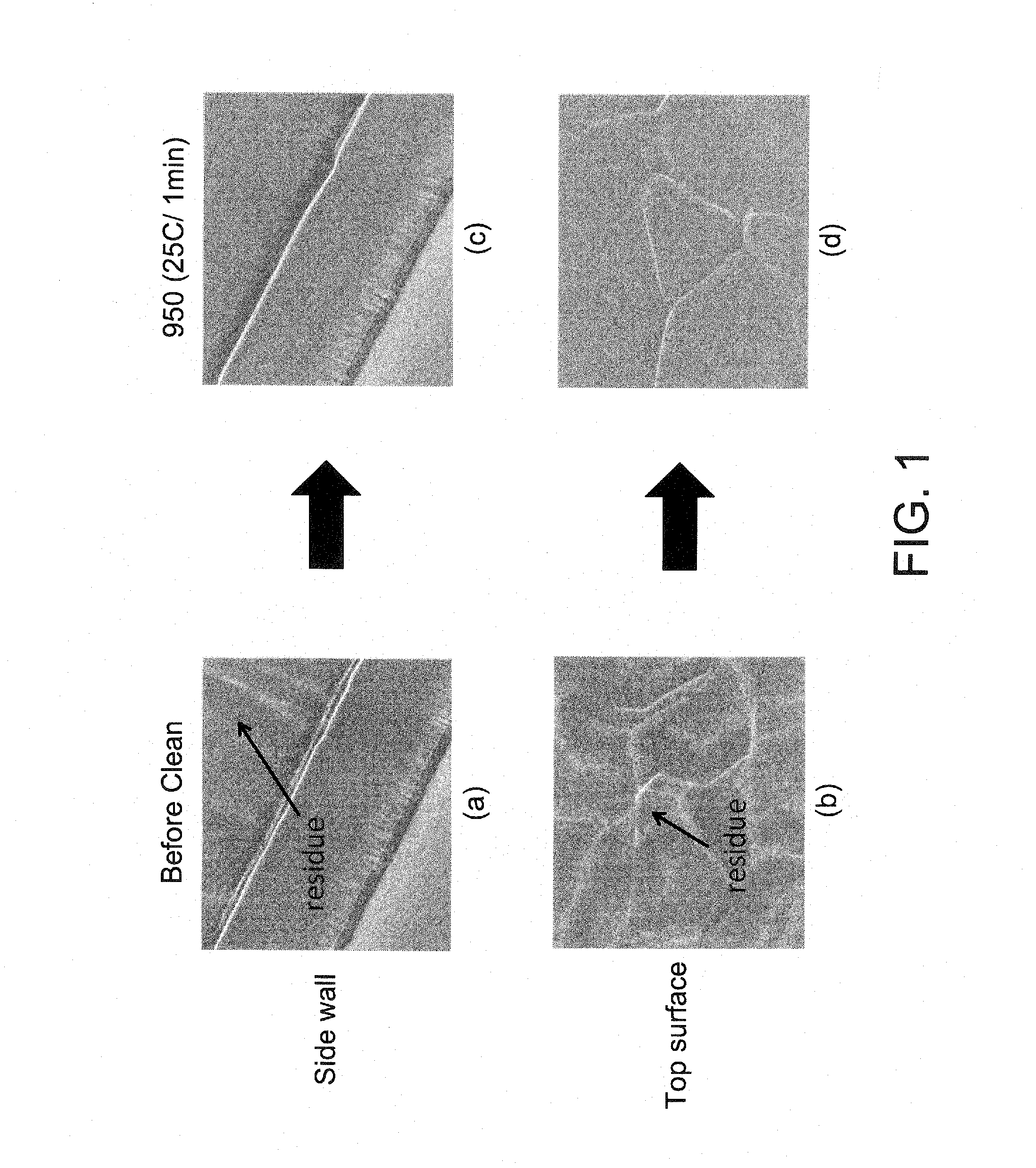
The present invention provides a composition for removing residue from a semiconductor substrate that includes water, a water-miscible organic solvent, an amine compound, an organic acid, and a fluoride ion source. The composition can be used in a cleaning process that involves contacting the substrate with the composition and rinsing it with water. Additionally, a replenishment composition can be added to the cleaning composition to restore the composition's effectiveness. The composition helps to remove residue without increasing the dielectric constant of the substrate.

Problems solved by technology

Such dry etching processes also typically render the resist mask extremely difficult to remove.
Finding a suitable cleaning composition for removal of this residue without adversely affecting, e.g., corroding, dissolving or dulling, the metal circuitry has also proven problematic.
Failure to completely remove or neutralize the residue can result in discontinuances in the circuitry wiring and undesirable increases in electrical resistance.
Unfortunately, shorter process times generally translates to more aggressive chemistries which can have a detrimental effect on the low-k dielectric material, as well as other stack materials (e.g., copper, etch stop, etc.).
Such prior art stripping compositions for removing the etching residue suffer, however, from significant drawbacks.
For example, their use tends to erode copper wire exposed on the bottoms of via holes.
Moreover, where porous interlayer low-k dielectrics are concerned, prior art stripping compositions either etch the porous interlayer dielectric materials or include components that adsorb into the pores thus increasing the dielectric constant, k, of the dielectric materials, which may potentially negatively impact the performance of the ultimate device.
Ether solvents, however, have the potential to damage the low-k layer.
Thus, ether solvents can contaminate the porous low-k layer and adversely affect its insulation ability.
In addition, ether solvents can adversely affect and increase the copper etch rate.

Method used


Image

  • Cleaning Formulations
  • Cleaning Formulations

Examples


examples

[0072]The following examples are provided for the purpose of further illustrating the present invention but are by no means intended to limit the same.

General Procedure for Preparing the Cleaning Compositions

[0073]All compositions which are the subject of the present Examples were prepared by mixing 500 g of material in a 600 mL beaker with a 1″ Teflon-coated stir bar.

Compositions of the Substrate

[0074]Each substrate used in the present Examples comprised an organosilicate glass (OSG) dielectric material with a titanium nitride capping layer that was deposited on a silicon nitride substrate. The OSG was etched by reactive ion etching (RIE) to leave behind OSG lines capped with titanium nitride. Following RIE, the substrates were treated in a plasma to ash the photoresist.

Processing Conditions

[0075]Cleaning tests were run using 305 mL of the cleaning compositions in a 400 mL beaker with a ½″ round Teflon stir bar set at 600 rpm. The cleaning compositions were heated to the desired te...


PUM

PropertyMeasurementUnit
dielectric constantaaaaaaaaaa
temperaturesaaaaaaaaaa

Abstract

A composition and method for removing copper-containing post-etch and / or post-ash residue from patterned microelectronic devices is described. The removal composition includes water, a water-miscible organic solvent, an amine compound, an organic acid, and a fluoride ion source. The compositions effectively remove the copper-containing post-etch residue from the microelectronic device without damaging exposed low-k dielectric and metal interconnect materials.

Description

CROSS-REFERENCE TO RELATED APPLICATIONS[0001]This nonprovisional application claims the benefit of U.S. Application No. 61 / 717,152, filed on Oct. 23, 2012, and U.S. Application No. 61 / 817,134, filed on Apr. 29, 2013, both provisional applications having the same title as the present application. U.S. Application Nos. 61 / 717,152 and 61 / 817,134 are hereby incorporated by reference in their entireties.BACKGROUND OF THE INVENTION[0002]The present invention relates to cleaning compositions that can be used for a variety of applications including, for example, removing unwanted resist films, post-etch, and post-ash residue on a semiconductor substrate. In particular, the present invention relates to cleaning compositions useful for the removal of residue, preferably copper-containing post-etch and / or post-ash residue, from the surface of substrates, preferably microelectronic devices, and methods of using said compositions for removal of same.[0003]The background of the present invention ...

Claims


Application Information

Patent Timeline
Patent Type & Authority Applications(United States)
IPC IPC(8): G03F7/42H01L21/02
CPCH01L21/02052G03F7/422C11D7/10C11D7/265C11D7/3209C11D7/3218C11D7/3281C11D7/5013C11D7/5022G03F7/425G03F7/426
Inventor LEE, YI CHIARAO, MADHUKAR BHASKARABANERJEE, GAUTAMLIU, WEN DARWU, AIPINGINAOKA, SEIJI
Owner VERSUM MATERIALS US LLC
Learn More