Filter chip element and method of preparing the same

a filter chip and filter chip technology, applied in the field of filter chip elements and a filter chip element preparation method, can solve the problems of difficult smooth processing of data, increased frequency of transmitting and receiving distortion, and delay in internal signal lines, so as to prevent noise and increase the magnetic permeability and impedance value

Active Publication Date: 2014-05-15
SAMSUNG ELECTRO MECHANICS CO LTD
View PDF5 Cites 7 Cited by
  • Summary
  • Abstract
  • Description
  • Claims
  • Application Information

AI Technical Summary

Benefits of technology

[0019]An object of the present invention is to provide a filter chip element that prevents noise in b

Problems solved by technology

When data is transmitted and received between a main device and a peripheral device at a high frequency band of GHz in order to transmit and receive a large amount of data, it is difficult to smoothly process the data due to signal delay and other interferences.
In particular, various port to port connections such as a communication line and an image and audio signal lines are used as in a digital TV, issues in terms of internal signal line delay and transmitting and receiving distortion may occur more frequently.
Conventional wound and stack type counter EMI components have large sizes of chip elements and low electrical properties, and thus, may be used only in a limited region of a large size circuit board.
A fired substrate may have different thicknesses at an edge portion and a central portion, may be bent, and may break or crack due to weak shock Thus, it is not appropriate to use the fired substrate as a ferrite substrate for EMI and electr

Method used


Image

  • Filter chip element and method of preparing the same
  • Filter chip element and method of preparing the same
  • Filter chip element and method of preparing the same

Examples


example 1

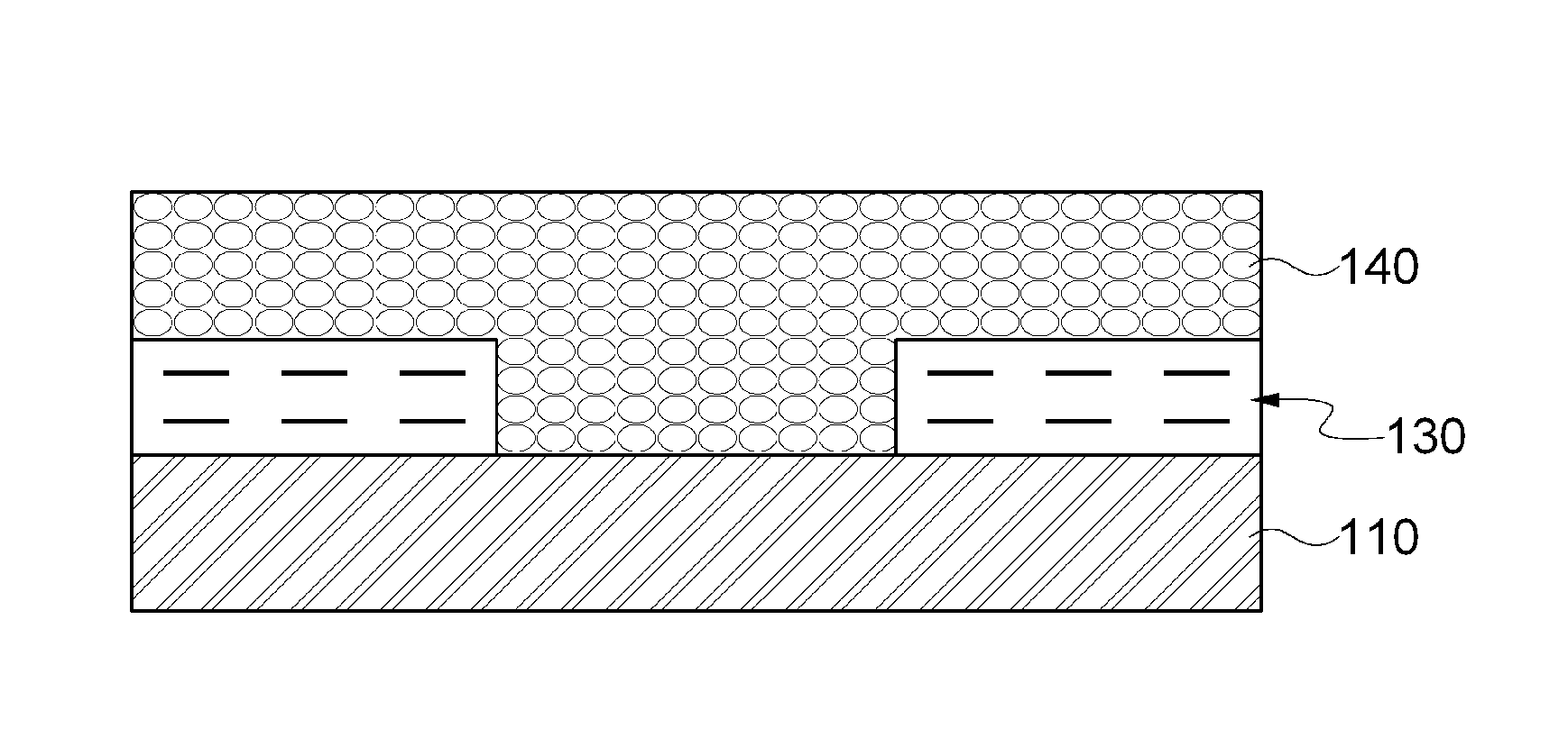
[0086]As shown in FIG. 3, primarily, foaming resin, NIPAM was impregnated on an upper or side surfaces of Cu internal coil patterns of a ferrite substrate whereon internal coil patterns are formed using Cu and was semi-hardened at a temperature of 130° C. to form pores in the foaming resin.

[0087]Spherical oxide powder (Fe oxide+Cu and Ni oxide, and average diameter of 5 to 45 μm) was inserted into the pores formed in the foaming resin by a squeeze with a ratio of foaming resin:oxide powder=30 wt %:70 wt %.

[0088]Then, the resultant was completely hardened at a temperature of 170° C. to prepare a filter chip element including a ferrite composite layer.

example 2

[0089]A filter chip element including a ferrite composite layer was prepared using the same manner as in Example 1 except that the filter chip element includes 10 wt % of silicon resin based on the foaming resin.

example 3

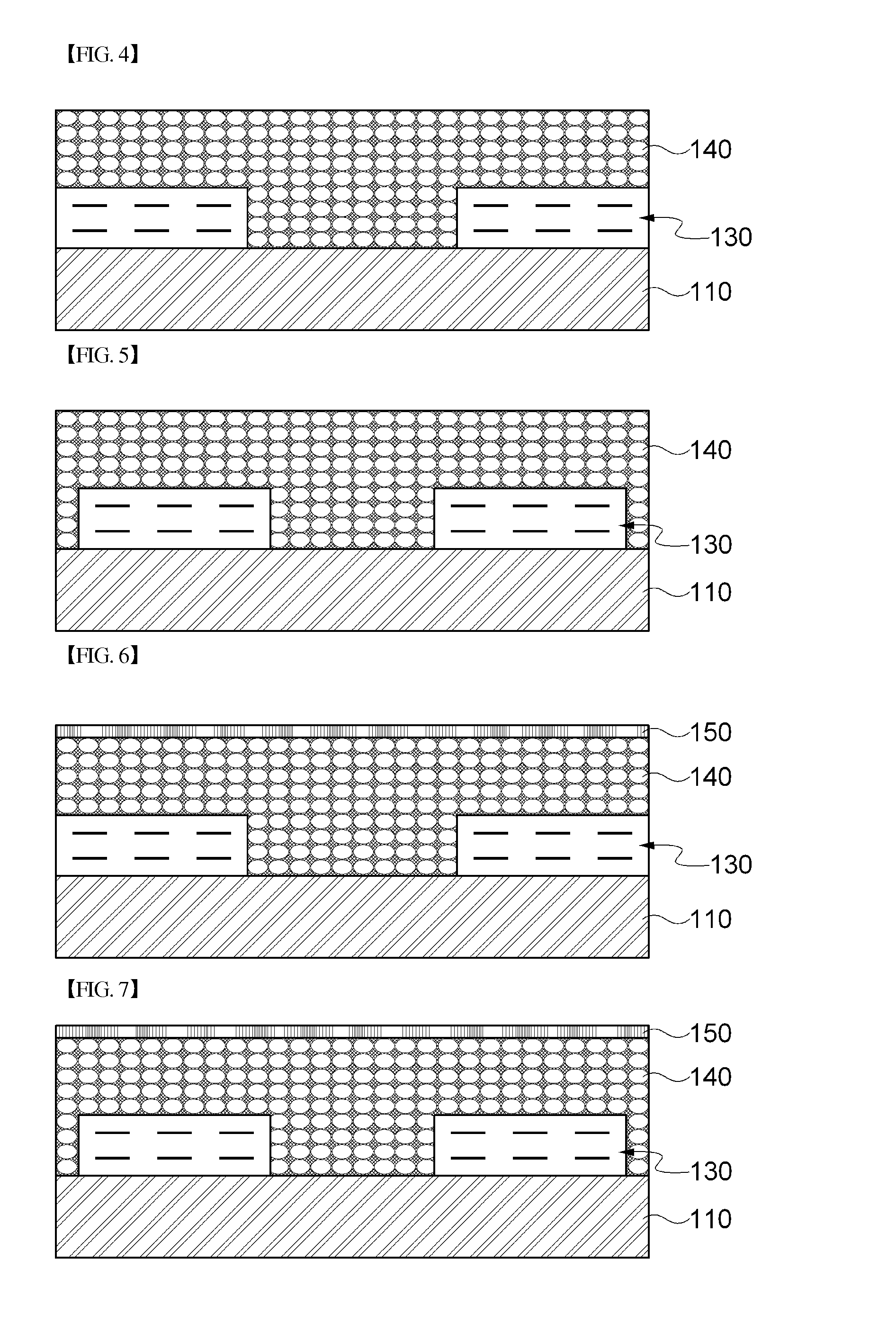
[0090]A filter chip element was prepared using the same manner as in Example 1 except that a reinforcing layer including 2 wt % of CNT powder based on foaming resin, having excellent electromagnetic shielding properties and excellent magnetic permeability was formed on the ferrite composite layer so as to have a structure shown in FIG. 7.


PUM


Abstract

Disclosed herein is a filter chip element including a ferrite substrate, internal coil patterns formed on the ferrite substrate; and a ferrite composite layer filled between the internal coil patterns formed on the ferrite substrate, wherein the ferrite composite layer includes foaming resin, thereby increasing magnetic permeability and a Q value which are important characteristics of a filter chip element for noise prevention among electromagnetic shielding components.

Description

CROSS REFERENCE(S) TO RELATED APPLICATIONS[0001]This application claims the benefit under 35 U.S.C. Section 119 of Korean Patent Application Ser. No. 10-2012-0128156, entitled “Filter Chip Element and Method of Preparing the Same” filed on Nov. 13, 2012, which is hereby incorporated by reference in its entirety into this application.BACKGROUND OF THE INVENTION[0002]1. Technical Field[0003]The present invention relates to a filter chip element and a method of preparing the same.[0004]2. Description of the Related Art[0005]Recently, data transmitting and receiving functions of an electronic device such as a digital television (TV), a smart phone, and a notebook computer at a high frequency band have been widely used. Also, in the future, it is expected that multifunctional and compound electronic devices formed by connecting electronic devices to each other via a universal serial bus (USB) or other communication ports as well as a single electronic device are highly used.[0006]In orde...

Claims


Application Information

Patent Timeline
IPC IPC(8): H03H7/01
CPCH03H7/0138H03H1/0007H01F2017/0093H01F17/0013H01F2017/0066H01F17/045H01F41/041
Inventor KIM, YONG SUKWI, SUNG KWONSHIN, HYEOG SOOLEE, SANG MOONYOO, YOUNG SEUCKPARK, SUNG JIN
Owner SAMSUNG ELECTRO MECHANICS CO LTD
Why Eureka
Try Eureka