Photovoltaic module

a photovoltaic module and photovoltaic technology, applied in the field of photovoltaic modules, can solve the problems of thermal damage to the photovoltaic cells, poor attachment workability of the bypass diode type, and lowering the generation of electricity per area, so as to prevent local concentration of current, reduce the generation of leakage paths in the diode part, and increase resistance

Inactive Publication Date: 2014-06-05
FUJI ELECTRIC CO LTD
View PDF0 Cites 6 Cited by
  • Summary
  • Abstract
  • Description
  • Claims
  • Application Information

AI Technical Summary

Benefits of technology

[0021]In the photovoltaic module according to the present invention, because the first electrode layer and/or the second electrode layer of the diode assembly is formed of a conductive oxide, and the conductive oxide is unlikely to diffuse mutually with Si, generation of a leak path in the diode part can be lowered.
[0022]Moreover, the conductive oxide has a greater resistance than Al or Ag. The use of the conductive oxide as an electrode material of the diode concentrates currents into a contact section betwee

Problems solved by technology

This might cause thermal damage to the photovoltaic cells.
However, this type of bypass diode has poor attachment workability because each of the mold diodes needs to be disposed in each of the photovoltaic cells.
Disposing the diodes outside the photovoltaic cells increases the area of a section not contributing to the generation of electricity, lowering the generation of electricity per area.
However, metals such as Al and Ag diffuse mutually with Si, and the amorphous silic

Method used


Image

  • Photovoltaic module
  • Photovoltaic module
  • Photovoltaic module

Examples


Embodiment Construction

[0030]An embodiment of the photovoltaic module according to the present invention is described with reference to FIGS. 1 to 6.

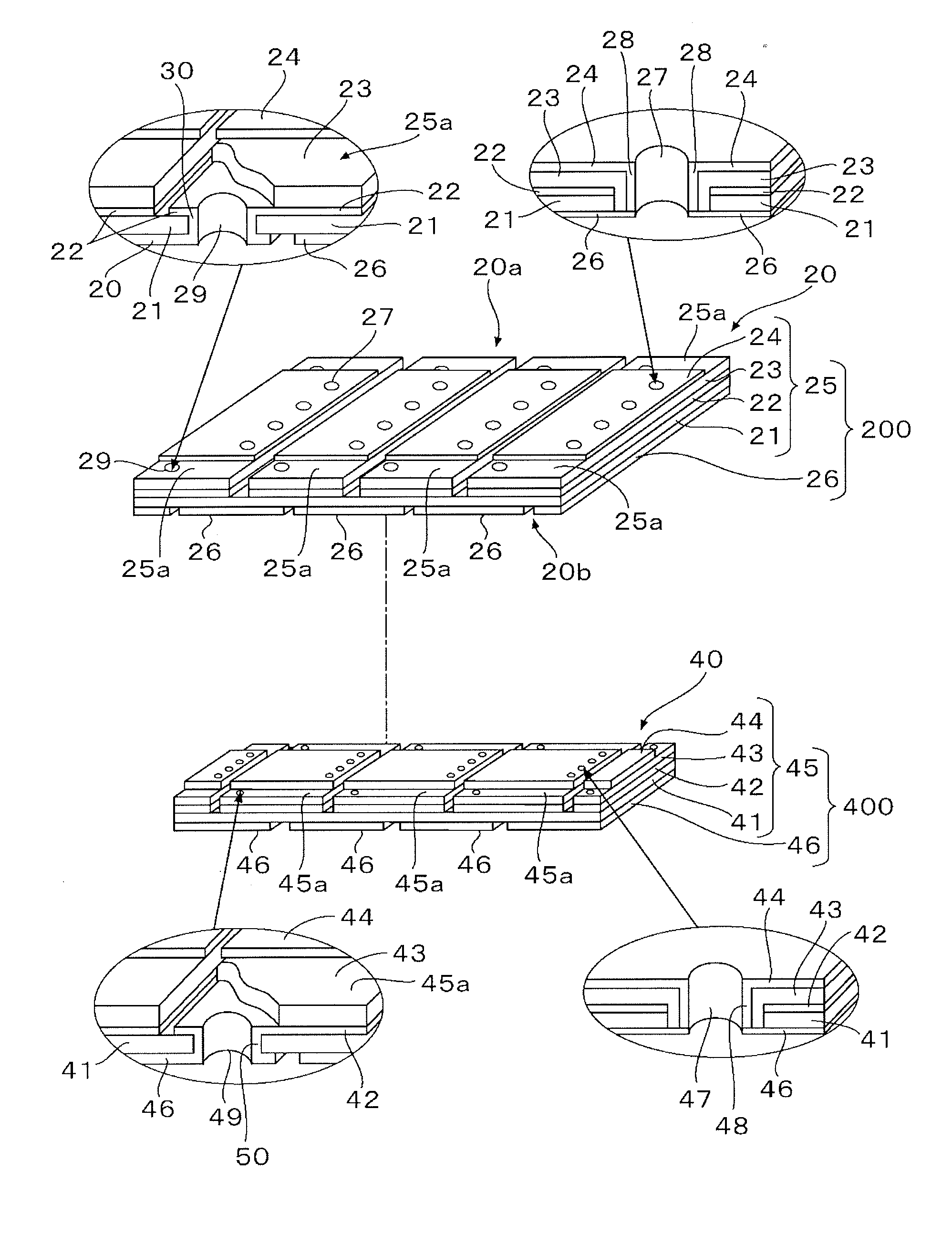
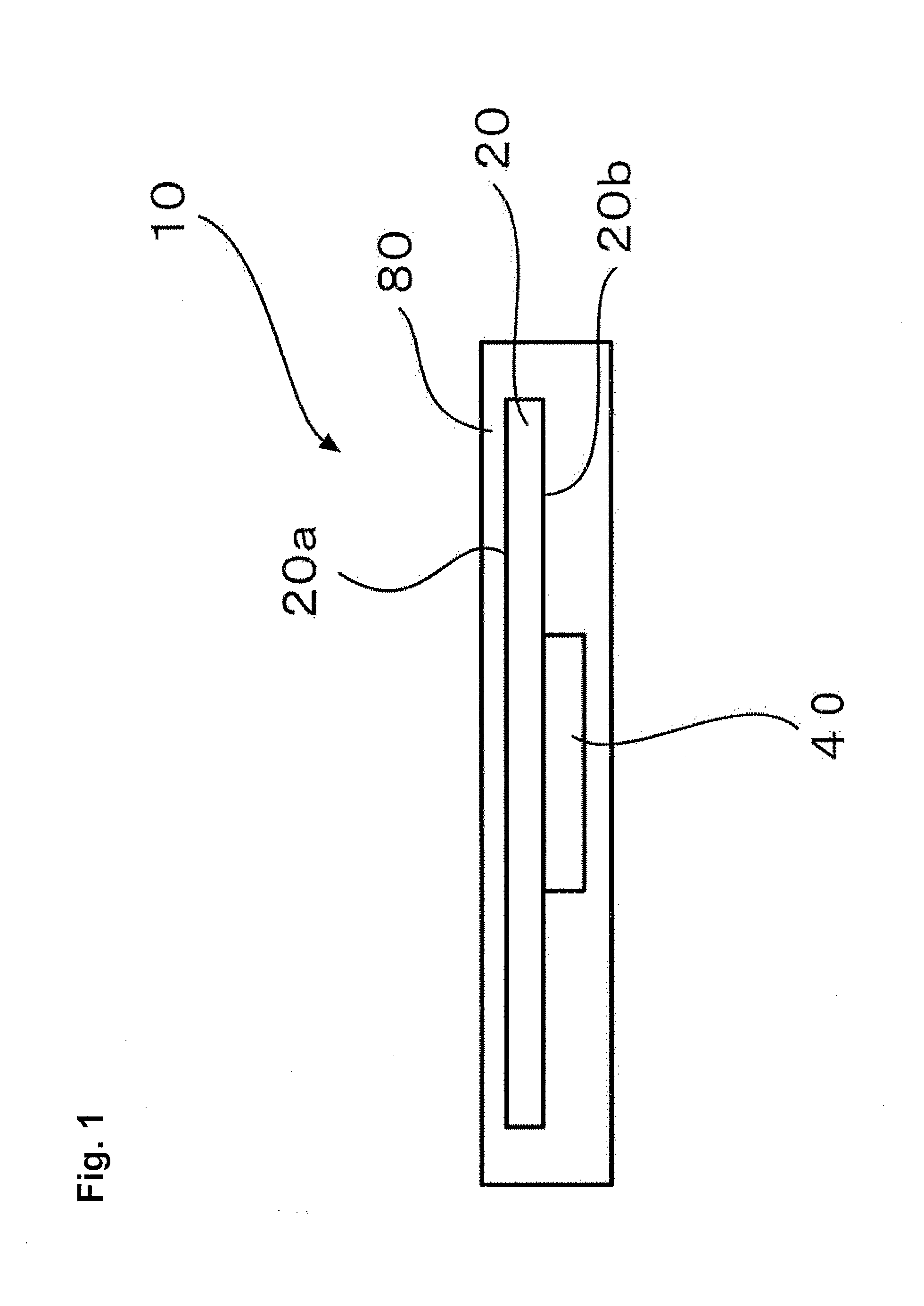
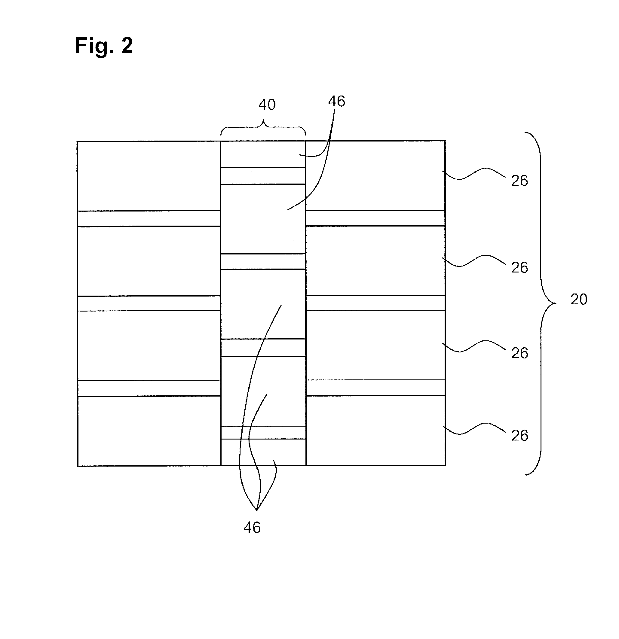
[0031]FIG. 1 is a schematic diagram showing a cross section of a photovoltaic module 10. FIG. 2 is a schematic diagram showing a bottom surface of the photovoltaic module 10. The photovoltaic module 10 is mainly configured by a photovoltaic cell assembly 20 and a diode assembly 40. The diode assembly 40 is configured such that an electrode layer of a non-light receiving surface 20b of the photovoltaic cell assembly 20 and an electrode layer of the diode assembly are pressure-bonded to each other, whereby these electrode surfaces surface-contact and are joined to each other. The diode assembly 40 and the photovoltaic cell assembly 20 are integrated and sealed by a sealing member 80. When viewing the bottom surface of the photovoltaic module 10, back surface electrode layers 26 (four, in FIG. 2) of photovoltaic unit cells constituting the photovoltaic cell asse...


PUM


Abstract

A photovoltaic module has a photovoltaic cell assembly and a diode assembly. The photovoltaic cell assembly is formed by stacking a rear surface electrode layer, a photoelectric conversion layer, and a transparent electrode layer on one surface of a substrate, and an electrode layer formed on the other surface of the substrate. The diode assembly is formed by sequentially stacking a first electrode layer, a semiconductor layer, and a second electrode layer on one surface of a second substrate. The first electrode layer or the second electrode layer of the diode assembly is formed of a conductive oxide. The electrode layer formed on the other surface of the substrate of the photovoltaic cell assembly and the electrode layer of the diode assembly surface-contact and electrically connected with each other. The photovoltaic cell assembly and the diode assembly are sealed and integrated with each other by a sealing member.

Description

TECHNICAL FIELD[0001]The present invention relates to a photovoltaic module with a bypass diode.BACKGROUND ART[0002]A photovoltaic module is designed by electrically connecting a plurality of photovoltaic cells in series to obtain a predetermined output.[0003]Incidentally, in a non-electricity generating state of a photovoltaic battery (when the sunlight irradiated to the photovoltaic battery is blocked), the resistance of photovoltaic cells increases, generating heat. This might cause thermal damage to the photovoltaic cells. In order to prevent such damage to the photovoltaic cells, the photovoltaic battery is provided with a bypass diode in which diodes are connected electrically in parallel to the photovoltaic cells and a current is bypassed from the diodes when a shadow or other problem occurs in part of the photovoltaic cells.[0004]In a standard bypass diode, mold diodes are connected to the outside of photovoltaic cells. However, this type of bypass diode has poor attachment ...

Claims


Application Information

Patent Timeline
IPC IPC(8): H01L27/142
CPCH01L27/1421H01L31/0465Y02E10/50
Inventor TSUJI, TAKETOWADA, TAKEHITO
Owner FUJI ELECTRIC CO LTD
Why Eureka
Try Eureka