Semiconductor device and method for manufacturing the same

Active Publication Date: 2014-06-26
SEMICON ENERGY LAB CO LTD
View PDF9 Cites 21 Cited by
  • Summary
  • Abstract
  • Description
  • Claims
  • Application Information

AI Technical Summary

Benefits of technology

[0035]According to one embodiment of the present invention, a semiconductor device including a capacitor whose charge capacity is increased while the aperture ratio is improved ca

Problems solved by technology

However, when the area of a light-blocking conductive film is increased to increase the area of a portion where a pair of el

Method used


Image

  • Semiconductor device and method for manufacturing the same
  • Semiconductor device and method for manufacturing the same
  • Semiconductor device and method for manufacturing the same

Examples


embodiment 1

[0091]In the present embodiment, a semiconductor device of one embodiment of the present invention is described with reference to drawings. Note that in this embodiment, a semiconductor device of one embodiment of the present invention is described with a liquid crystal display device taken as an example.

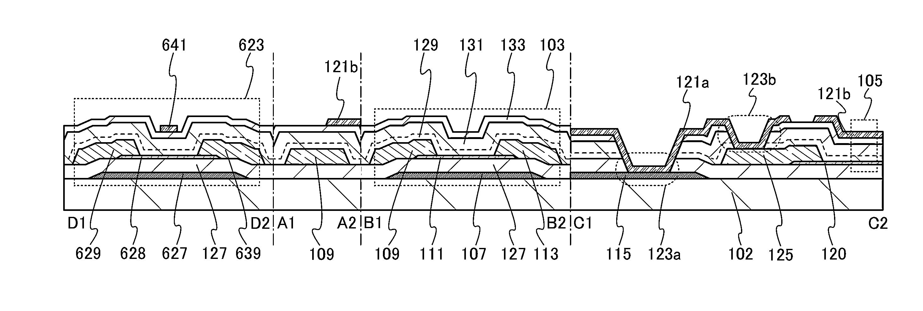
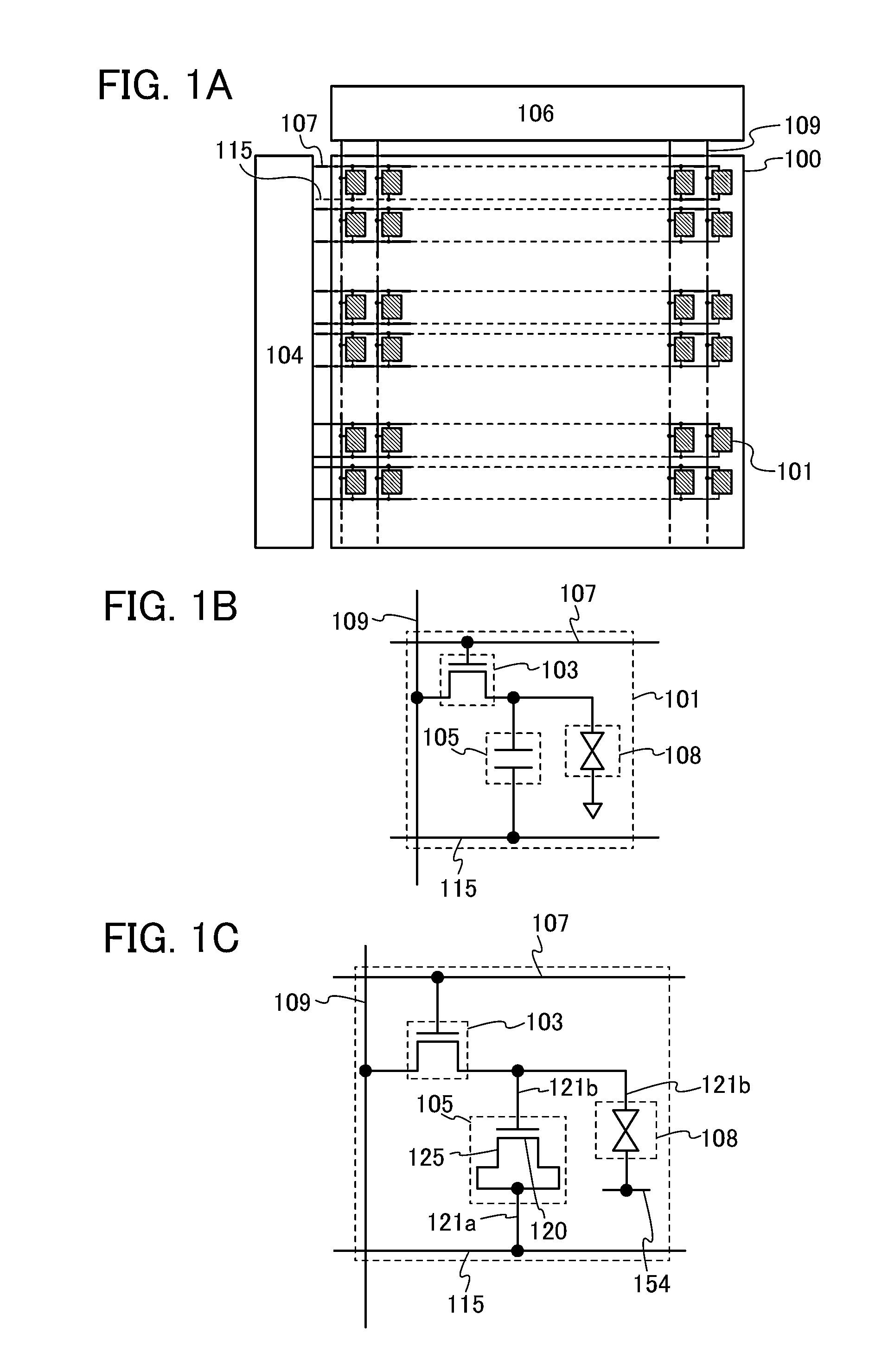
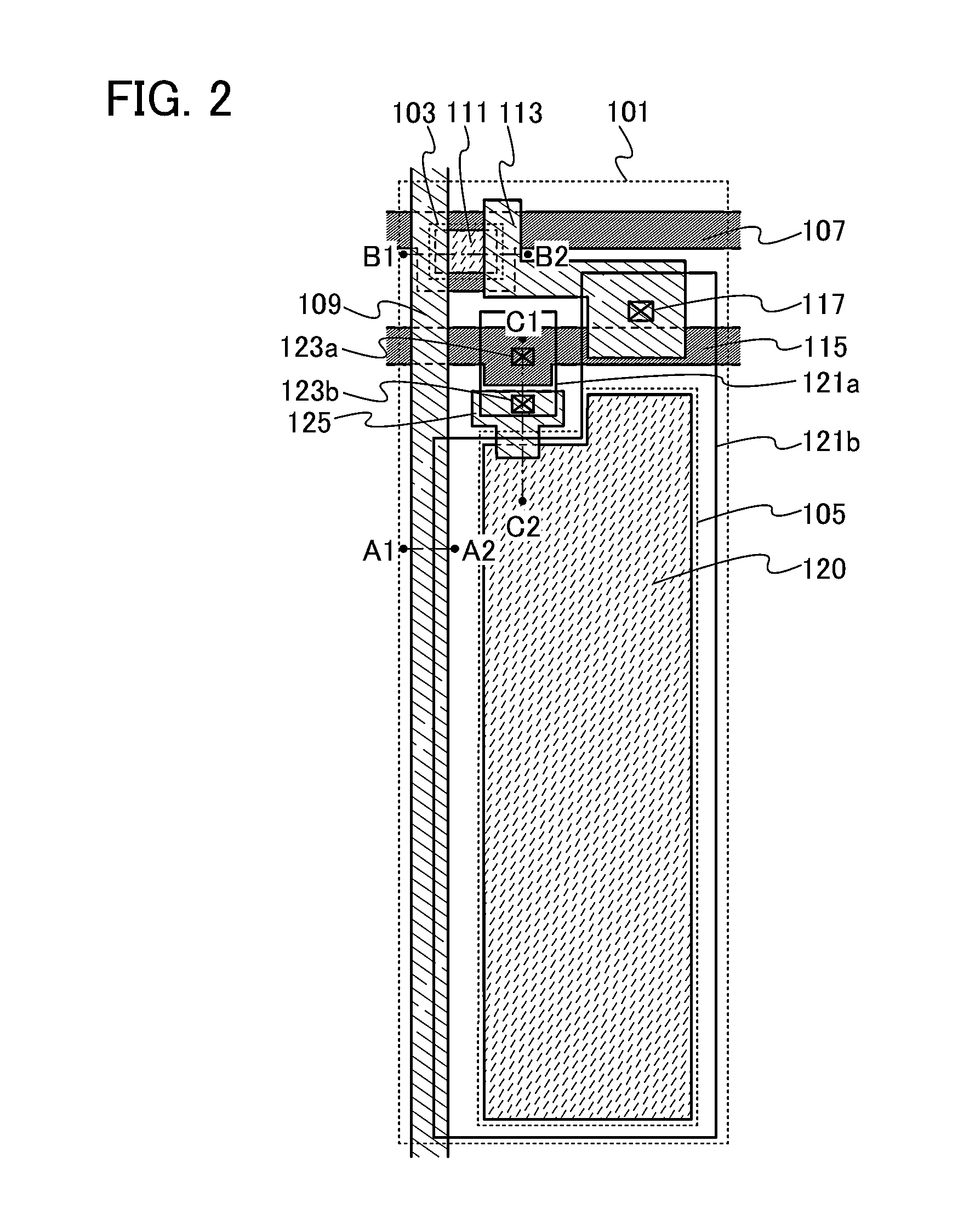
[0092]FIG. 1A illustrates an example of a semiconductor device. The semiconductor device illustrated in FIG. 1A includes a pixel portion 100, a scan line driver circuit 104, a signal line driver circuit 106, m scan lines 107 which are arranged in parallel or almost in parallel and whose potentials are controlled by the scan line driver circuit 104, and n signal lines 109 which are arranged in parallel or almost in parallel and whose potentials are controlled by the signal line driver circuit 106. Further, the pixel portion 100 includes a plurality of pixels 101 arranged in a matrix. Capacitor lines 115 which are arranged in parallel or almost in parallel to the scan lines 107 are al...

modification example 1

[0196]In the semiconductor device of one embodiment of the present invention, the top shape of the conductive film 125 which electrically connects the capacitor line 115 and the conductive film 120 serving as one electrode of the capacitor 105 can be changed as appropriate. For example, in order to reduce contact resistance between the conductive film 120 and the conductive film 125, the conductive film 125 can be provided in contact with the conductive film 120 along the outer edge thereof. The conductive film 125 is formed in a formation process which is the same as that of the signal line 109 including the source electrode of the transistor 103 and the conductive film 113 including the drain electrode of the transistor 103 and thus may have a light-blocking property; for this reason, the conductive film 125 is preferably formed into a loop shape.

modification example 2

[0197]Although in the pixel 101 described above, the transistor in which the semiconductor film is located between the gate insulating film and the signal line 109 including the source electrode and the conductive film 113 including the drain electrode is used, instead of the transistor, a transistor in which a semiconductor film is provided between the insulating film 129, and a signal line including a source electrode and a conductive film including a drain electrode can be used.


PUM


Abstract

A semiconductor device in which the aperture ratio and which includes a capacitor with increased charge capacity is provided. A semiconductor device in which the number of masks used in a manufacturing process is reduced and the manufacturing costs are reduced is also provided. An impurity is contained in a light-transmitting semiconductor film so that the semiconductor film functions as one of a pair of electrodes in a capacitor. The other pair of electrodes is formed using a light-transmitting conductive film such as a pixel electrode. Further, a scan line and a capacitor line are provided on the same surface and in parallel to each other. An opening reaching the capacitor line and an opening reaching a conductive film which can be formed in the formation of a source electrode or a drain electrode of the transistor can be formed concurrently in an insulating film.

Description

BACKGROUND OF THE INVENTION[0001]1. Field of the Invention[0002]The present invention relates to a product (including a machine, a manufacture, and a composition of matter) and a process (including a simple process and a production process). In particular, one embodiment of the present invention relates to a semiconductor device, a display device, a light-emitting device, and a power storage device, to a method for driving the same, and to a method for manufacturing the same. In particular, one embodiment of the present invention relates to a semiconductor device including an oxide semiconductor, a display device including an oxide semiconductor, or a light-emitting device including an oxide semiconductor.[0003]2. Description of the Related Art[0004]In recent years, flat panel displays such as liquid crystal displays (LCDs) have been widespread. In each of pixels provided in the row direction and the column direction in a display device such as a flat panel display, for example, a t...

Claims


Application Information

Patent Timeline
IPC IPC(8): H01L27/12
CPCH01L27/1259H01L27/1255H01L27/1225G02F1/1368H01L27/124H01L29/786
Inventor YAMAZAKI, SHUNPEIMIYAKE, HIROYUKI
Owner SEMICON ENERGY LAB CO LTD
Why Eureka
Try Eureka