Compound semiconductor ESD protection devices

a protection device and semiconductor technology, applied in semiconductor devices, semiconductor/solid-state device details, electrical apparatus, etc., can solve problems such as device degradation or damage, and lack of good esd protection devices, and achieve the effect of greatly reducing the size of the chip

Active Publication Date: 2014-07-03
WIN SEMICON
View PDF3 Cites 5 Cited by
  • Summary
  • Abstract
  • Description
  • Claims
  • Application Information

AI Technical Summary

Benefits of technology

[0006]The main object of the present invention is to provide a compound semiconductor ESD protection device using a multi-gate E-FET with at least one of the gates connected to the source, the drain or a region between two adjacent gates. The total device area can be made smaller than an ESD protection device using plural series connected single-gate E-FET diodes. The chip size is greatly reduced when the ESD protection device is integrated in a compound semiconductor circuit to be protected.

Problems solved by technology

An integrated circuit (IC) connected to external terminals is vulnerable to electrostatic discharge (ESD) pulses from the operating environment and peripherals such as human bodies or machines.
An ESD event may produce high current or high voltage pulses within a few nanoseconds, leading to device degradation or damage.
However, the lack of good ESD protection devices has become a major drawback in HEMT switch applications.
With increasing number of diodes connected in series in the same direction and / or the opposite direction, the area occupied by the whole ESD protection device becomes large, which results in the increase in the total chip size.

Method used


Image

  • Compound semiconductor ESD protection devices
  • Compound semiconductor ESD protection devices
  • Compound semiconductor ESD protection devices

Examples


Embodiment Construction

Type I Compound Semiconductor ESD Protection Device

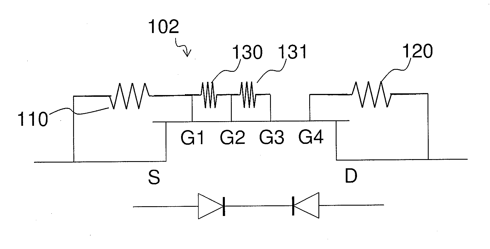
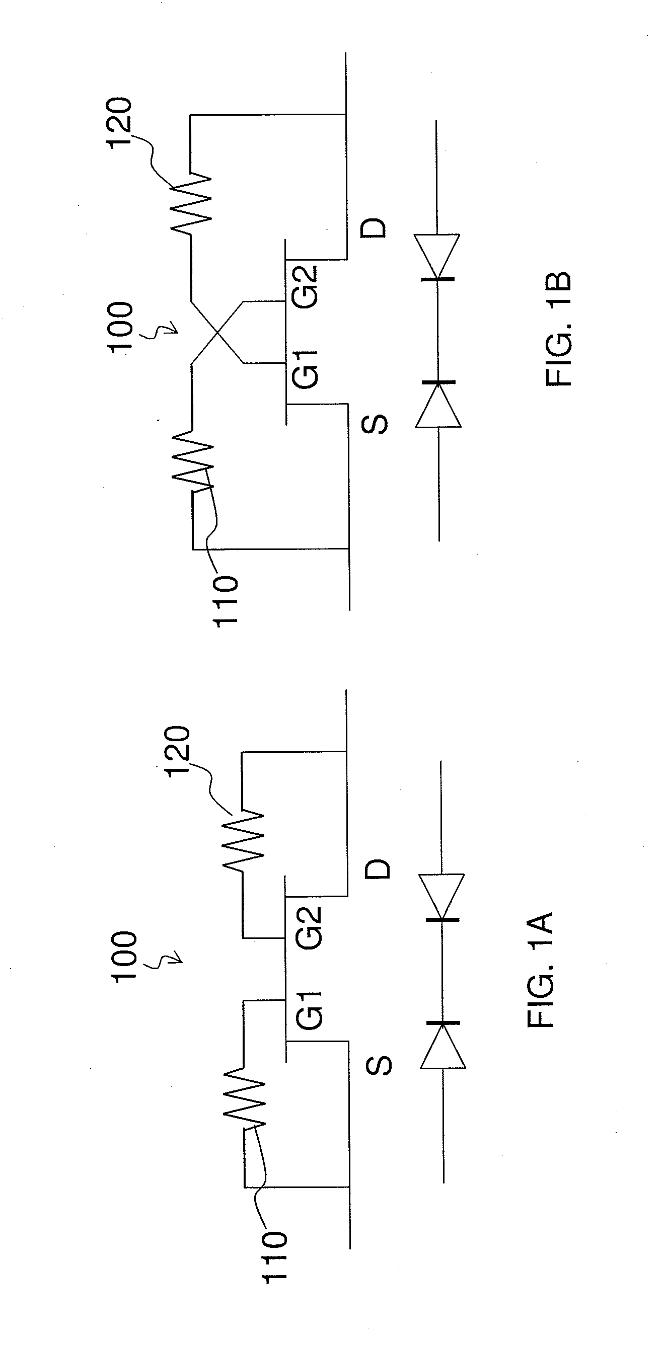
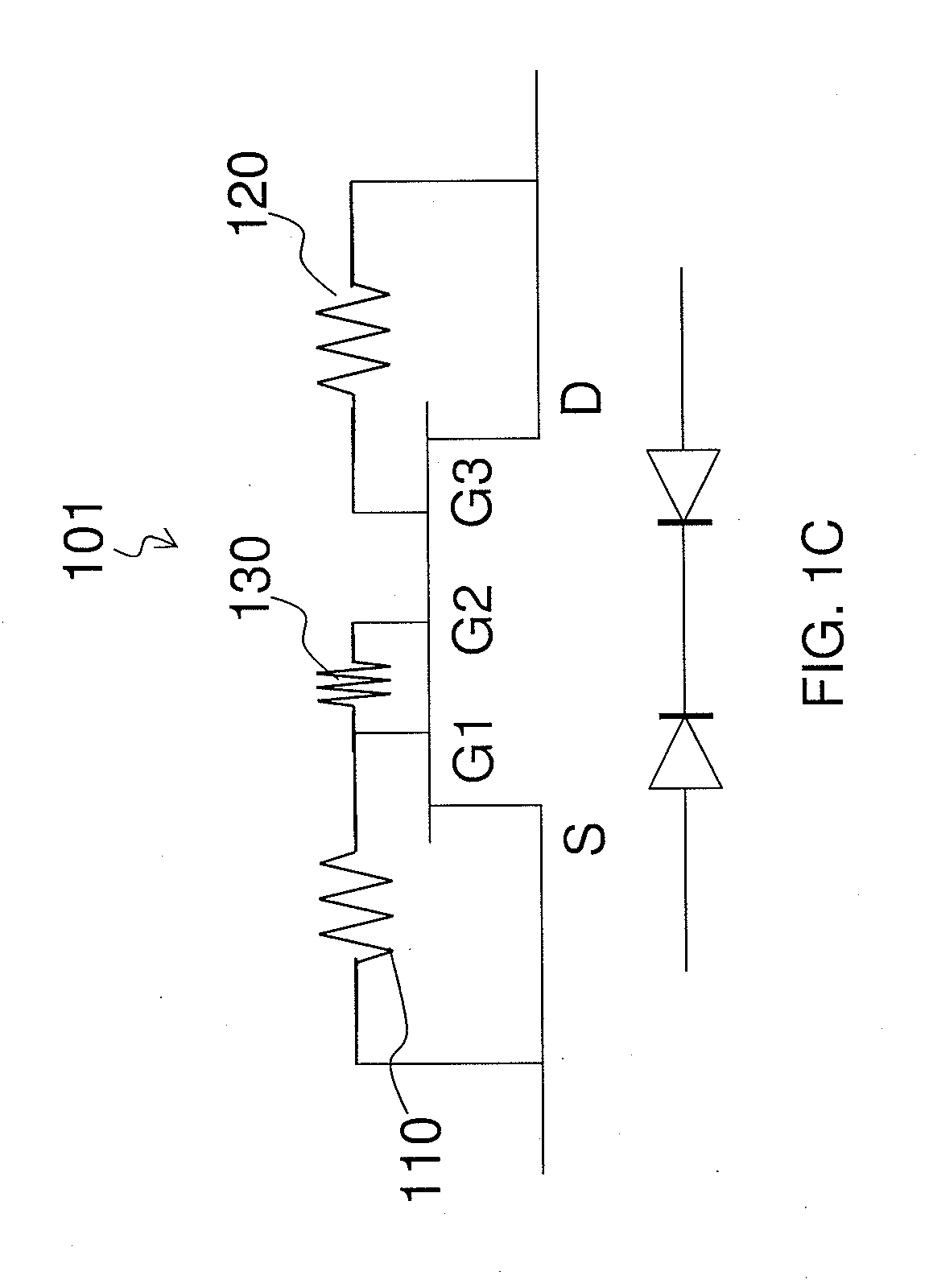
[0030]FIG. 1A˜1E are circuit diagrams showing embodiments of the type I compound semiconductor ESD protection device provided by the present invention. The type I compound semiconductor ESD protection device is equivalent to a circuit having two diodes connected in opposite directions. The type I compound semiconductor ESD protection device comprises a multi-gate E-FET (100˜102), at least one first resistor 110, and at least one second resistor 120. The multi-gate E-FET comprises a source electrode S, a drain electrode D, and plural gate electrodes (G1˜G4) disposed between the source and drain electrodes. The source electrode S is connected to at least one of the plural gate electrodes through the at least one first resistor 110, and the drain electrode is connected to at least one of the plural gate electrodes through the at least one second resistor 120. In these embodiments, the type I ESD compound semiconductor protection device...


PUM


Abstract

The present invention relates to compound semiconductor ESD protection devices of three types. The device comprises a multi-gate enhancement mode FET (E-FET). For the type I compound semiconductor ESD protection device, the source electrode is connected to the plural gate electrodes through at least one first resistor, and the drain electrode is connected to the plural gate electrodes through at least one second resistor. For the type II compound semiconductor ESD protection device, the plural gate electrodes are connected to at least one of the inter-gate regions between two adjacent gate electrodes through at least one fourth resistor. For the type III compound semiconductor ESD protection device, the plural gate electrodes are connected to the source or drain electrodes through at least one seventh resistor. Any two gate electrodes in the three types of compound semiconductor ESD protection devices can be connected by a resistor.

Description

FIELD OF THE INVENTION[0001]The present invention relates to compound semiconductor devices, and more particularly, to compound semiconductor electrostatic discharge protection devices.BACKGROUND OF THE INVENTION[0002]An integrated circuit (IC) connected to external terminals is vulnerable to electrostatic discharge (ESD) pulses from the operating environment and peripherals such as human bodies or machines. An ESD event may produce high current or high voltage pulses within a few nanoseconds, leading to device degradation or damage. In order to protect the vulnerable IC from ESD damaging pulses, an ESD protection circuit has to be connected to the external terminals of main IC elements.[0003]Compound semiconductor devices have been widely used in the radio frequency (RF) circuits market. For example, compound semiconductor high electron mobility transistor (HEMT) switch have been widely applied in 3G cell phone applications in recent year for their high performance in RF range. How...

Claims


Application Information

Patent Timeline
Patent Type & Authority Applications(United States)
IPC IPC(8): H01L29/20H01L27/04
CPCH01L27/04H01L29/2003H01L27/0266H01L29/778
Inventor TAKATANI, SHINICHIROCHUNG, JUNG-TAOWANG, CHI-WEIYUAN, CHENG-GUANLIU, SHIH-MING JOSEPH
Owner WIN SEMICON
Why Eureka
Try Eureka