Compound semiconductor ESD protection devices

a protection device and compound semiconductor technology, applied in semiconductor devices, semiconductor/solid-state device details, electrical apparatus, etc., can solve problems such as device degradation or damage, lack of good esd protection devices, and circuits connected to external terminals, and achieve the effect of significantly improving manufacturing process and greatly reducing the size of compound semiconductor ic modules

Active Publication Date: 2014-07-03
WIN SEMICON
View PDF5 Cites 14 Cited by
  • Summary
  • Abstract
  • Description
  • Claims
  • Application Information

AI Technical Summary

Benefits of technology

[0004]The main object of the present invention is to provide a compound semiconductor ESD protection device using plural compound semiconductor E-FETs or a compound semiconductor multi-gate E-FET, so that the ESD protection circuits for a compound semicon...

Problems solved by technology

An integrated circuit (IC) connected to external terminals is vulnerable to electrostatic discharge (ESD) pulses from the operating environment and peripherals such as human bodies or machines.
An ESD event may produce high current or high voltage pulses within a few nanoseconds, leading to device degradation or damage.
However, the lack of g...

Method used


Image

  • Compound semiconductor ESD protection devices
  • Compound semiconductor ESD protection devices
  • Compound semiconductor ESD protection devices

Examples


Embodiment Construction

1. ESD Protection Devices Using Plural Single-Gate E-FETs

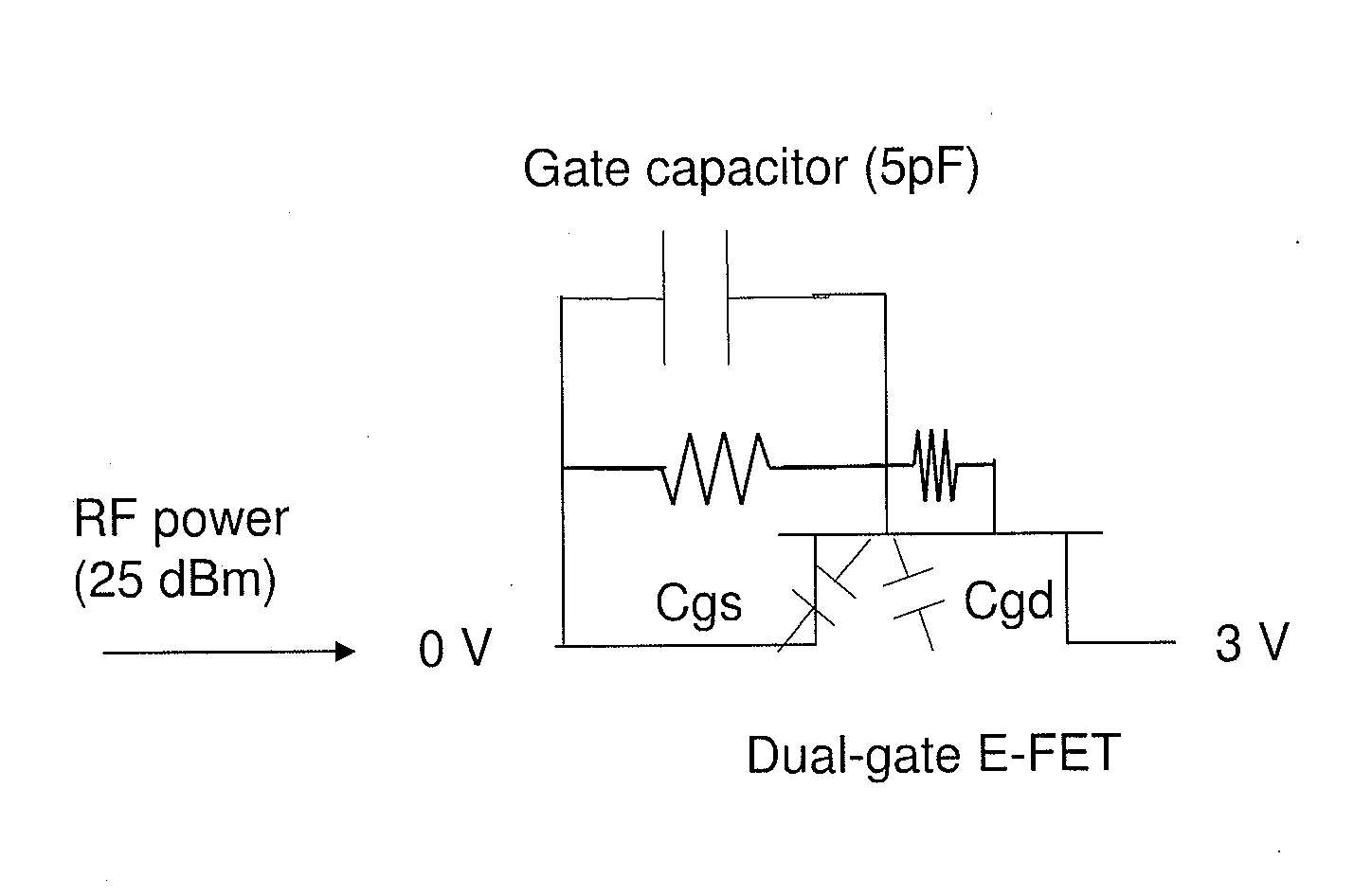
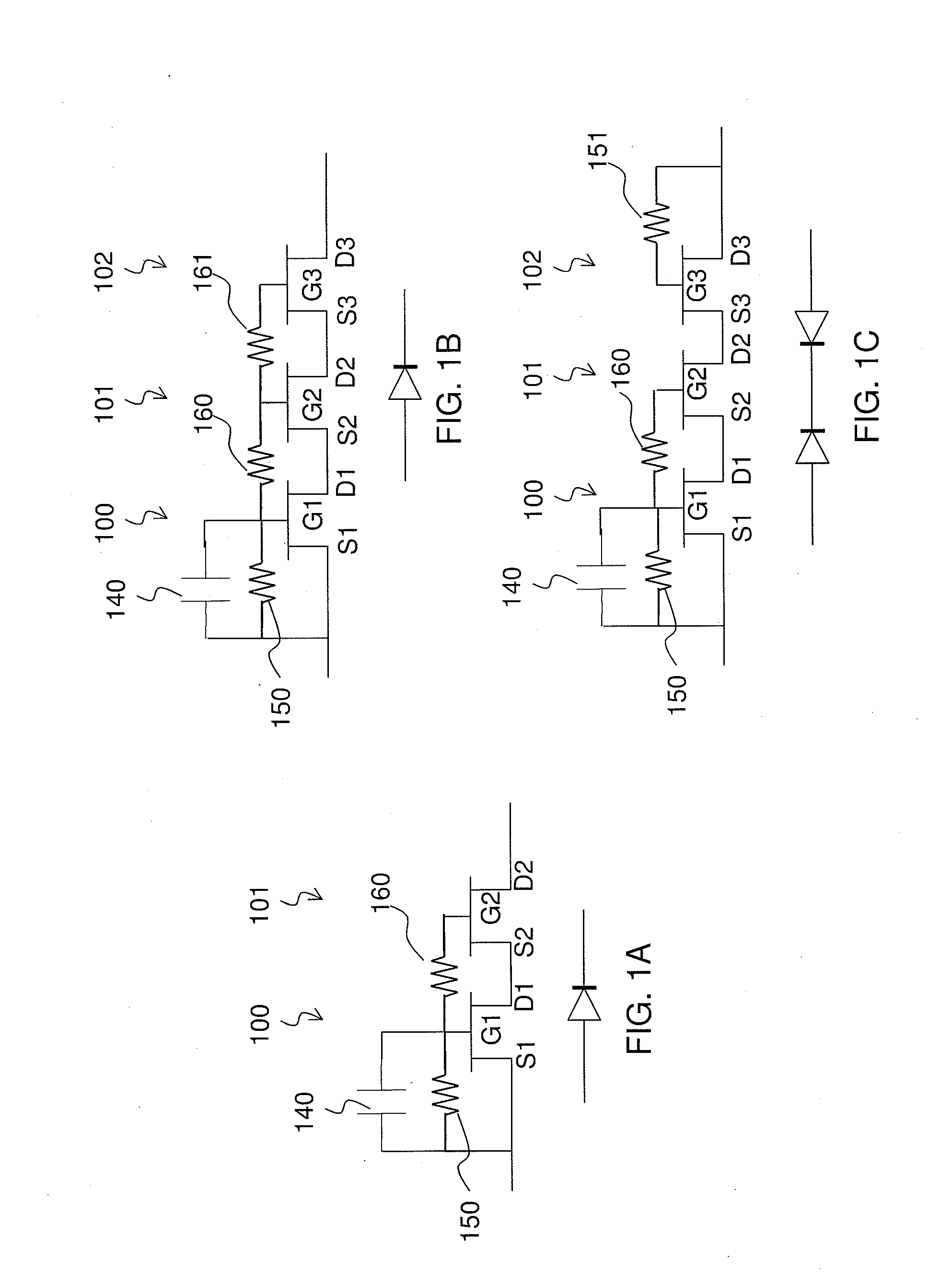
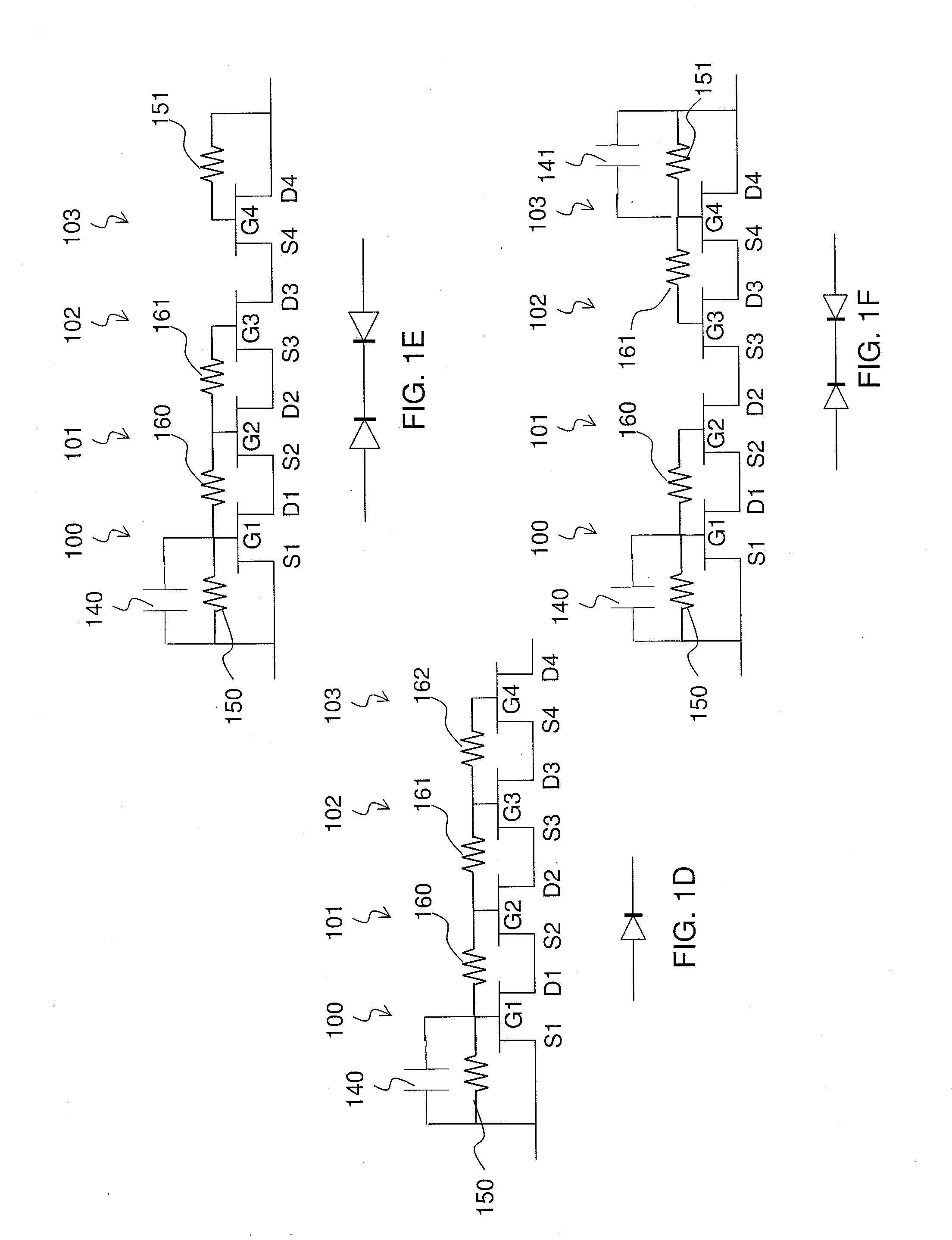
[0029]FIG. 1A˜1G are circuit diagrams showing the embodiments of a compound semiconductor ESD protection device using plural single-gate E-FETs provided by the present invention. An equivalent diode or diodes connection is shown on the bottom of each figure. The ESD protection device comprises plural single-gate E-FETs (100˜103), at least one first resistor (150 and 151), and at least one gate capacitor (140 and 141). The ESD protection device may further include at least one second resistor (160˜162) for connecting the gate electrodes of two single-gate E-FETs. Each of the plural single-gate E-FETs comprises a source electrode (S), a drain electrode (D), and a gate electrode (G). The plural single-gate E-FETs are connected in series. The drain electrode of a single-gate E-FET is connected to the source electrode of a succeeding single-gate E-FET. The gate electrode of each of the plural single-gate E-FETs is DC-connected the ...


PUM


Abstract

The present invention relates to compound semiconductor ESD protection devices using plural compound semiconductor E-FETs or compound semiconductor multi-gate E-FETs. The device comprises plural compound semiconductor E-FETs or multi-gate E-FETs, in which each of the gates is DC-connected to the source, drain, or an inter-gate region between two adjacent gates in the multi-gate E-FET through at least one first resister, and at least one of the gates is AC-connected to the source, drain, or an inter-gate region between two adjacent gates in the multi-gate E-FET through a gate capacitor.

Description

FIELD OF THE INVENTION[0001]The present invention relates to compound semiconductor devices, and more particular to compound semiconductor electrostatic discharge protection devices.BACKGROUND OF THE INVENTION[0002]An integrated circuit (IC) connected to external terminals is vulnerable to electrostatic discharge (ESD) pulses from the operating environment and peripherals such as human bodies or machines. An ESD event may produce high current or high voltage pulses within a few nanoseconds, leading to device degradation or damage. In order to protect the vulnerable IC from ESD damaging pulses, an ESD protection circuit has to be connected to the external terminals of main IC elements.[0003]Compound semiconductor devices have been widely used in the radio frequency (RF) circuits market. For example, compound semiconductor high electron mobility transistor (HEMT) switches have been widely applied in 3G cell phone applications in recent year for their high performance in RF range. Howe...

Claims


Application Information

Patent Timeline
IPC IPC(8): H01L23/60
CPCH01L23/60H01L27/0266H01L29/41758H01L29/42316H01L29/778H01L27/0248
Inventor TAKATANI, SHINICHIROCHUNG, JUNG-TAOWANG, CHI-WEIYUAN, CHENG-GUANLIU, SHIH-MING JOSEPH
Owner WIN SEMICON
Why Eureka
Try Eureka