
MRAM with Sidewall Protection and Method of Fabrication

a sidewall protection and memory technology, applied in the field of magnetic random access memory (mram), can solve the problems of destroying the functionality of the device, electrical short, and electrical short between the top and bottom electrodes during fabrication, and achieve the effect of high selectivity

Active Publication Date: 2014-07-31
AVALANCHE TECH
View PDF5 Cites 29 Cited by
  • Summary
  • Abstract
  • Description
  • Claims
  • Application Information

AI Technical Summary

Benefits of technology

Prevents electrical shorts and enhances fabrication yields by protecting the sidewalls during via etching, allowing for higher reliability and consistency in the interconnect process even with variations in etching depth, and addresses thickness variations in inter-layer dielectric layers.

Problems solved by technology

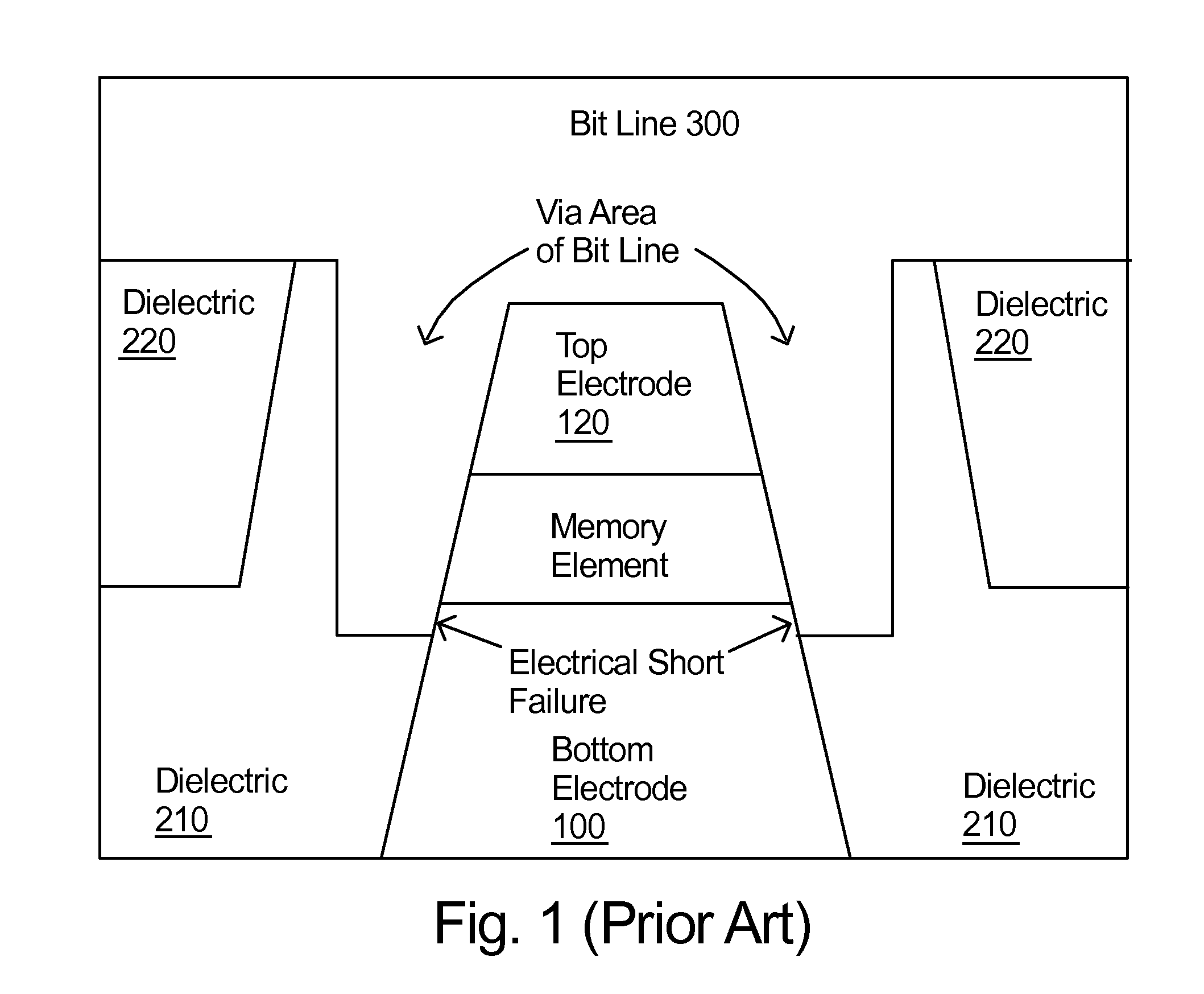
Herein arises a problem with the prior art that can result in an electrical short being formed between the top and bottom electrodes during fabrication.
If the etching of the via reaches to the sidewall of the bottom electrode, then the subsequent metal deposition in the bit line interconnect process causes a short between the top electrode to the bottom electrode, thereby destroying the functionality of the device.
Therefore, an electrical short that could happen when the via etch reaches down to the level of the barrier layer is a severe issue in this device.

Method used


Image

  • MRAM with Sidewall Protection and Method of Fabrication
  • MRAM with Sidewall Protection and Method of Fabrication
  • MRAM with Sidewall Protection and Method of Fabrication

Examples


Embodiment Construction

[0020]In the following description of the embodiments, reference is made to the accompanying drawings that form a part hereof, and in which is shown by way of illustration of specific embodiments in which the invention may be practiced. It is to be understood that other embodiments may be utilized without departing from the scope of the present invention. It should be noted that the figures discussed herein are not drawn to scale and thicknesses of lines are not indicative of actual sizes. The cross section view in the figures is generally taken through the approximate center the memory cell in a plane perpendicular to the substrate except where otherwise noted. Although only one cell is shown in the figures, the method may used for the simultaneous fabrication of a many cells on a wafer according to standard techniques.

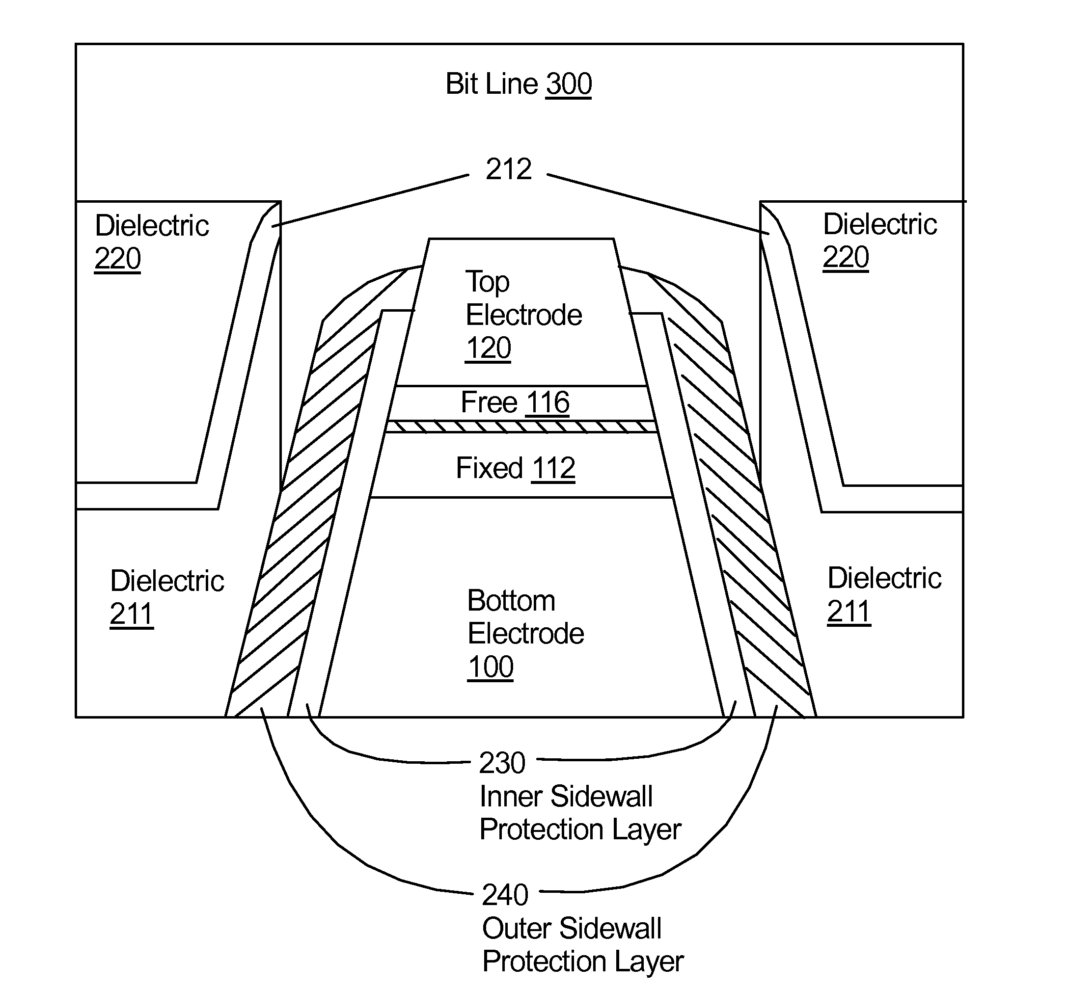
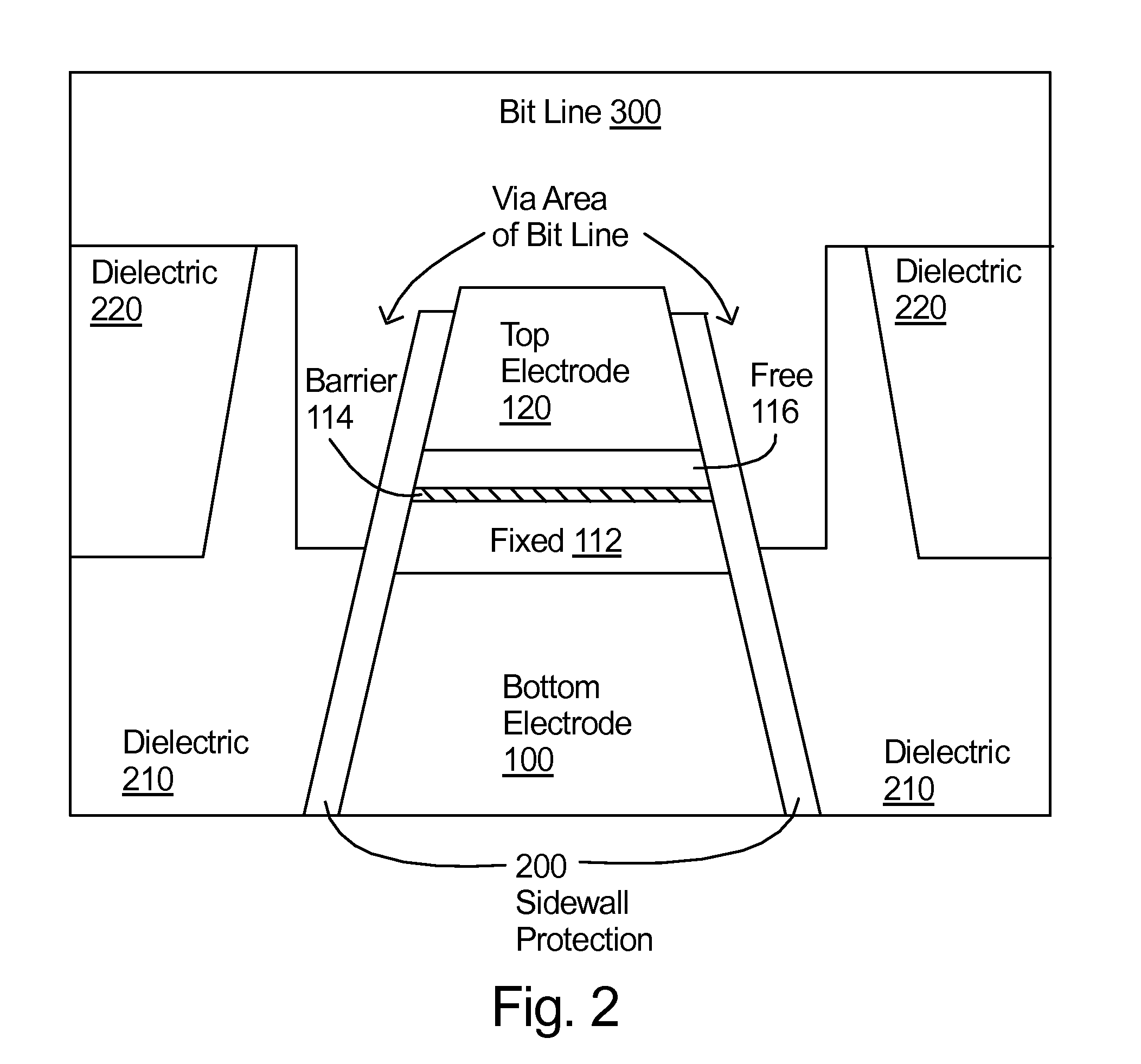
[0021]FIG. 2 illustrates a cross sectional view of a completed memory cell according to a first embodiment of the invention wherein the sidewalls of the memory eleme...


PUM


Abstract

BEOL memory cells are described that include one or more sidewall protection layers on the memory device (including, for example, an MTJ element) deposited prior to interconnect via etching to prevent the formation of electrical shorts between layers. One embodiment uses a single layer sidewall protection sleeve that is deposited after the memory device has been patterned. The layer material is vertically etched down to expose the upper surface of the top electrode while leaving a residual layer of protective material surrounding the rest of the memory device. The material for the protection layer is selected to resist the etchant used to remove the first dielectric material from the via in the subsequent interconnect process. A second embodiment uses dual-layer sidewall protection in which the first layer covers the memory element is preferably an oxygen-free dielectric and the second layer protects the first layer during via etching. In either the first or second embodiments a single layer or a dual layer etch stop layer structure can be deposited over the wafer after the sidewall protection sleeve has been formed and before the inter-layer dielectric (ILD) is deposited.

Description

CROSS REFERENCE TO RELATED APPLICATIONS[0001]This application is a divisional of co-pending U.S. patent application bearing Ser. No. 13 / 317,564 with filing date of Oct. 20, 2011, which is hereby incorporated by reference and which is a Continuation-In-Part of co-pending U.S. patent application bearing Ser. No. 13 / 136,454 with filing date of Aug. 1, 2011, which is also hereby incorporated by reference.FIELD OF THE INVENTION[0002]The present invention relates generally to semiconductor Back-End-Of-Line (BEOL) memories and particularly to Magnetic Random Access Memory (MRAM) and particularly to protecting the memory elements from being shorted during the interconnect process.DESCRIPTION OF THE PRIOR ART[0003]The BEOL memories such as RRAM (Resistive Random Access Memory), PRAM (Phase Change Random Access Memory), MRAM have a resistive device as a memory element. Because high speed access and non-volatility at power off are promised by these devices, they may replace existing memories a...

Claims


Application Information

Patent Timeline
Patent Type & Authority Applications(United States)
IPC IPC(8): H01L23/522H10B12/00
CPCH01L23/5226H01L2924/0002H10N50/01H10N50/10H01L2924/00H10B61/00H10B63/80H10N70/20H10N70/063H10N70/231H10N70/826
Inventor SATOH, KIMIHIROHUAI, YIMINGZHANG, JINGABEDIFARD, EBRAHIM
Owner AVALANCHE TECH
Learn More