
Broadband, Group Index Independent, and Ultra-Low Loss Coupling into Slow Light Slotted Photonic Crystal Waveguides

a photonic crystal waveguide and low loss technology, applied in the direction of optical waveguide light guide, instruments, etc., can solve the problems of reducing optical confinement, increasing propagation loss for slow light modes, weakening some benefits derived from slow light effects, etc., to achieve efficient coupling of light into slow light waveguide devices, high sensitivity for greenhouse gas detection, and efficient and easy fabrication design

Active Publication Date: 2014-08-07
BOARD OF RGT THE UNIV OF TEXAS SYST
View PDF1 Cites 8 Cited by
  • Summary
  • Abstract
  • Description
  • Claims
  • Application Information

AI Technical Summary

Benefits of technology

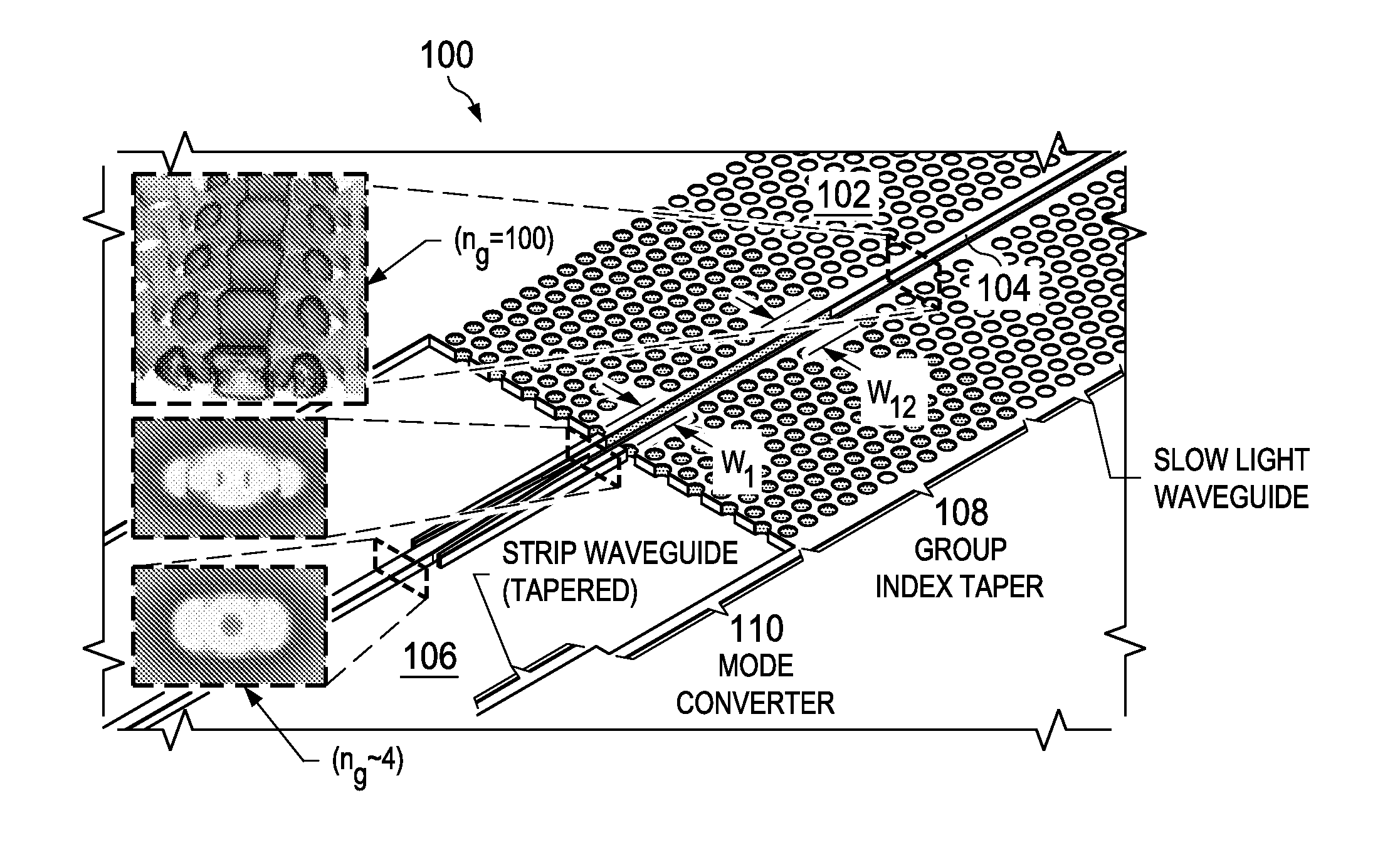
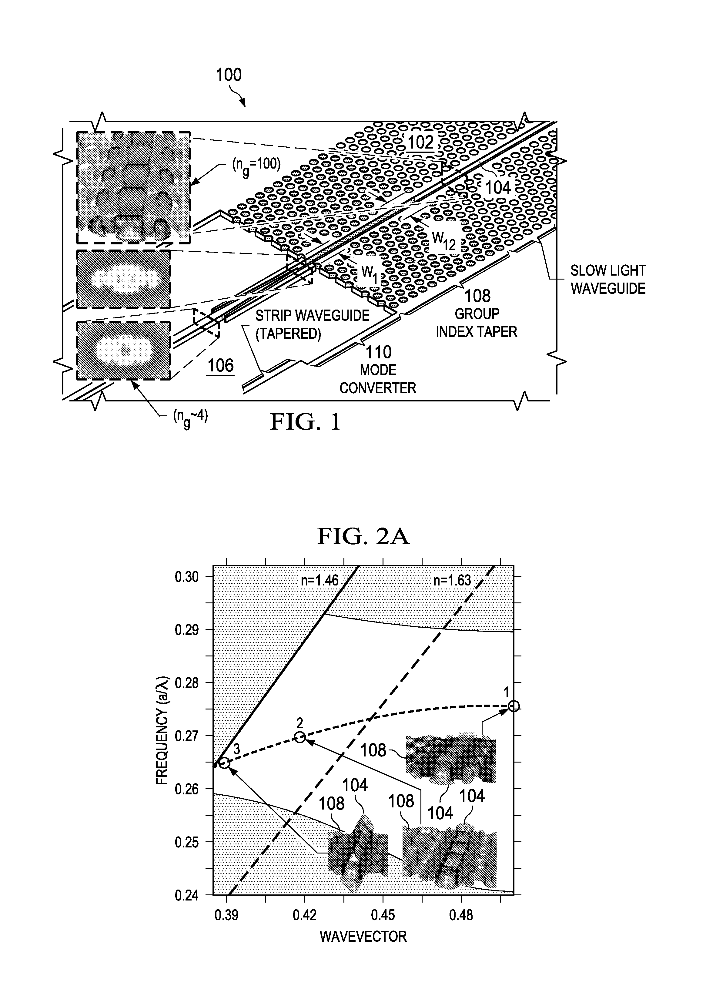
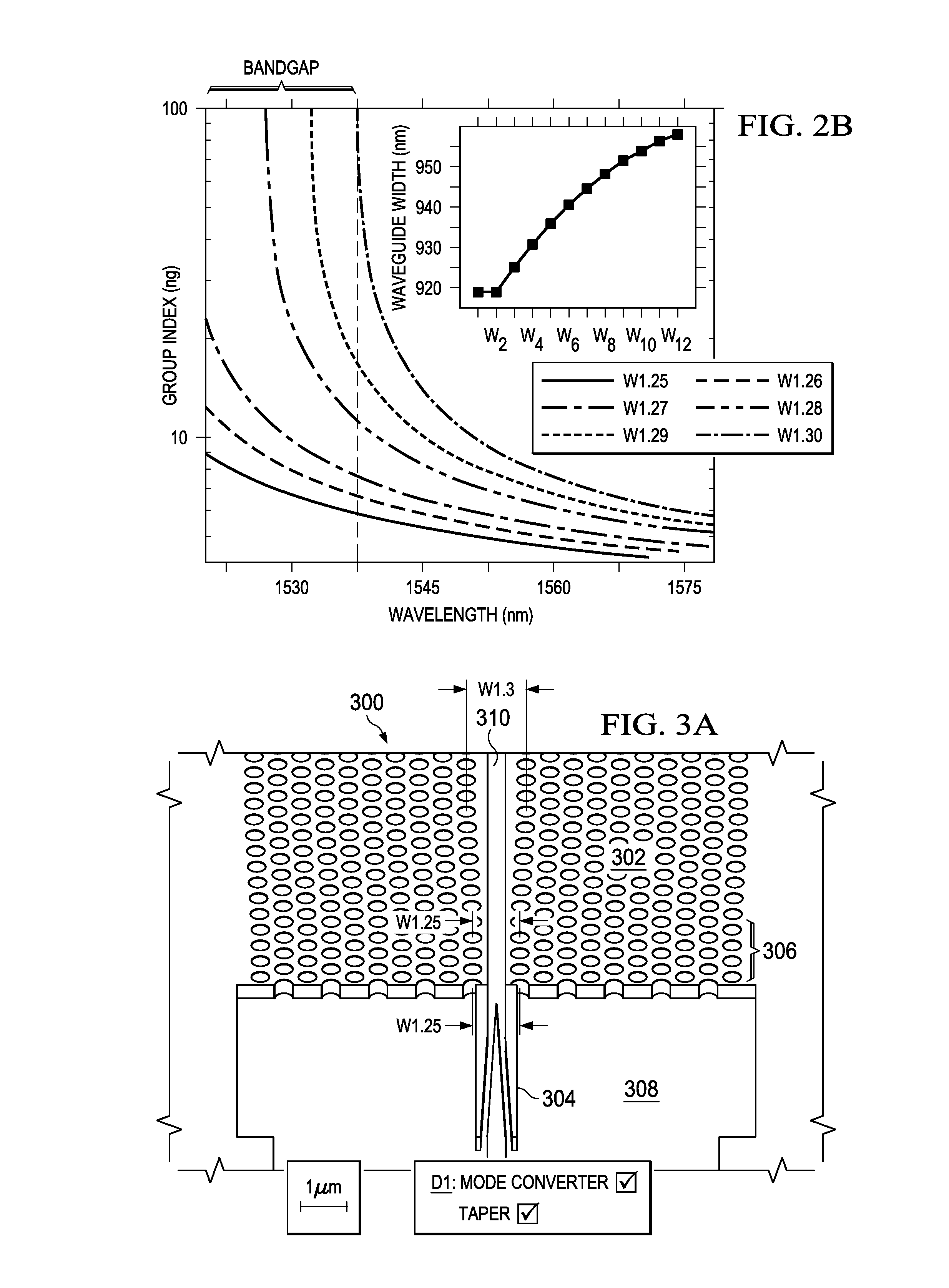
The present invention is about an efficient way to couple light into slow light waveguide devices. It has applications in optical communication systems and environmental sensors. It has several features that differ from existing designs, including a parabolic taper of slotted photonic crystal waveguide, an optical mode converter, and an efficient and easy to fabricate design. The invention improves the coupling efficiency with the slow light slotted photonic crystal waveguide by 30 dB. It is a simple, robust, and experimentally proven design, and it can be fabricated with high yield. The invention comprises an ultra-compact group index taper and an ultra-compact optical mode converter.

Problems solved by technology

[3] This lateral spread reduces optical confinement and increases propagation loss for slow light modes, which can weaken some of the benefits derived from the slow light effect.
Despite the benefits derived from strong confinement and slow light enhancement, optical coupling between a strip waveguide and a slotted PCW is more challenging than conventional PCW due to the exotic mode profile and slow group velocity in the slotted PCW.
Without a properly designed interface between a strip waveguide and a slotted PCW, strongly confined guided mode profile with minimal overlap and large group index mismatch result in negligible coupling and a transmission spectrum that is nearly indistinguishable from noise [9].
However, efficient coupling is achieved only within a narrow bandwidth.
Changing the slot termination profile achieves good coupling with significantly better bandwidth [10], but the overall transmission is low, and Fabry-Perot fringes manifest due to significant reflections.
However, the transmission dip below −10 dB in slow light region weakens the performance of slow light devices.
However, optical loss in photonic crystal waveguides is the most significant stumbling block, and coupling loss in photonic crystal devices is the dominant optical loss.

Method used


Image

  • Broadband, Group Index Independent, and Ultra-Low Loss Coupling into Slow Light Slotted Photonic Crystal Waveguides
  • Broadband, Group Index Independent, and Ultra-Low Loss Coupling into Slow Light Slotted Photonic Crystal Waveguides
  • Broadband, Group Index Independent, and Ultra-Low Loss Coupling into Slow Light Slotted Photonic Crystal Waveguides

Examples


Embodiment Construction

[0022]While the making and using of various embodiments of the present invention are discussed in detail below, it should be appreciated that the present invention provides many applicable inventive concepts that can be embodied in a wide variety of specific contexts. The specific embodiments discussed herein are merely illustrative of specific ways to make and use the invention and do not delimit the scope of the invention.

[0023]To facilitate the understanding of this invention, a number of terms are defined below. Terms defined herein have meanings as commonly understood by a person of ordinary skill in the areas relevant to the present invention. Terms such as “a”, “an” and “the” are not intended to refer to only a singular entity, but include the general class of which a specific example may be used for illustration. The terminology herein is used to describe specific embodiments of the invention, but their usage does not delimit the invention, except as outlined in the claims.

[...


PUM


Abstract

The present invention provides a waveguide coupler configured to optically couple a strip waveguide to a first slot photonic crystal waveguide, wherein the slot photonic crystal waveguide has a lattice constant, an air hole diameter, a slot width and a first line defect waveguide width. The waveguide coupler includes a group reflective index taper having a second slot photonic crystal waveguide disposed between and aligned with the first slot photonic crystal waveguide and the strip waveguide. The second slot photonic crystal waveguide has a length, the lattice constant, the air hole diameter, the slot width, and a second line defect waveguide width that is substantially equal to the first line defect waveguide width adjacent to the first slot photonic crystal waveguide and decreases along the length of the second photonic crystal waveguide.

Description

STATEMENT OF FEDERALLY FUNDED RESEARCH[0001]This invention was made with U.S. Government support under Contract Nos. FA 9550-08-1-0394 and FA 9550-09-C-0086 awarded by the Air Force Office of Scientific Research (AFOSR). The government has certain rights in this invention.TECHNICAL FIELD OF THE INVENTION[0002]The present invention relates in general to the field of ultra-compact optical devices, and more particularly, to an approach to efficiently couple light into slow light waveguide devices by the design of a slotted photonic crystal waveguide.REFERENCE TO A SEQUENCE LISTING[0003]None.BACKGROUND OF THE INVENTION[0004]Without limiting the scope of the invention, its background is described in connection with photonic crystal waveguides (PCW). Introducing line defects into a photonic crystal lattice permits an electromagnetic wave having a frequency within the bandgap of the structure to be guided through the photonic crystal. The line defects resemble waveguides, and may be formed...

Claims


Application Information

Patent Timeline
Patent Type & Authority Applications(United States)
IPC IPC(8): G02B6/26G02B6/10G02B6/14
CPCG02B6/26G02B6/14G02B2006/121G02B2006/1213G02B6/10G02B6/1225B82Y20/00
Inventor CHEN, RAY T.LIN, CHE-YUN
Owner BOARD OF RGT THE UNIV OF TEXAS SYST
Learn More