
pHEMT and HBT integrated epitaxial structure

a high electron mobility, integrated technology, applied in the direction of transistors, electrical devices, semiconductor devices, etc., can solve the problems of reducing current density, generating more lattice dislocations and defects, and generating higher lattice strain, so as to improve electron mobility in the channel, reduce resistance, and improve the effect of electron mobility

Inactive Publication Date: 2014-08-21
WIN SEMICON
View PDF2 Cites 11 Cited by
  • Summary
  • Abstract
  • Description
  • Claims
  • Application Information

AI Technical Summary

Benefits of technology

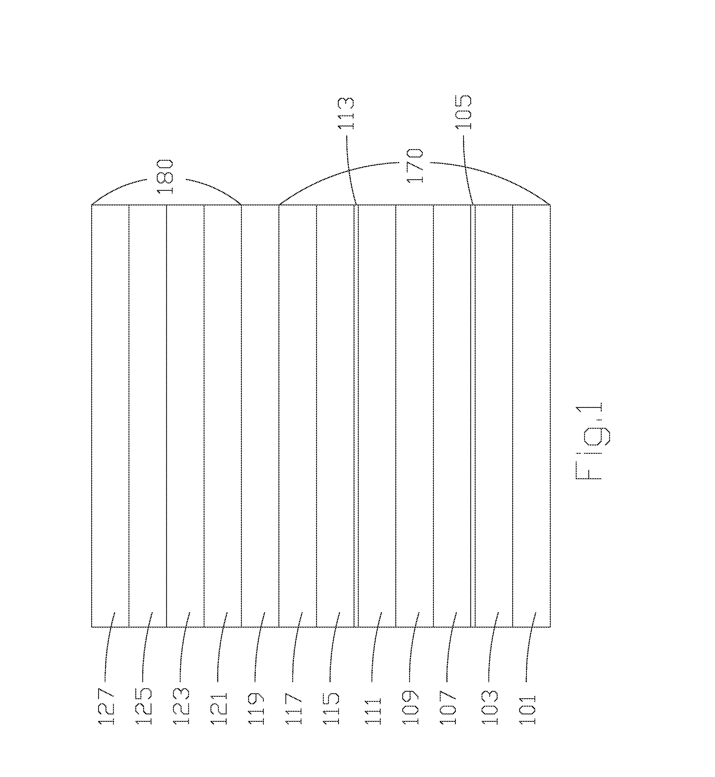
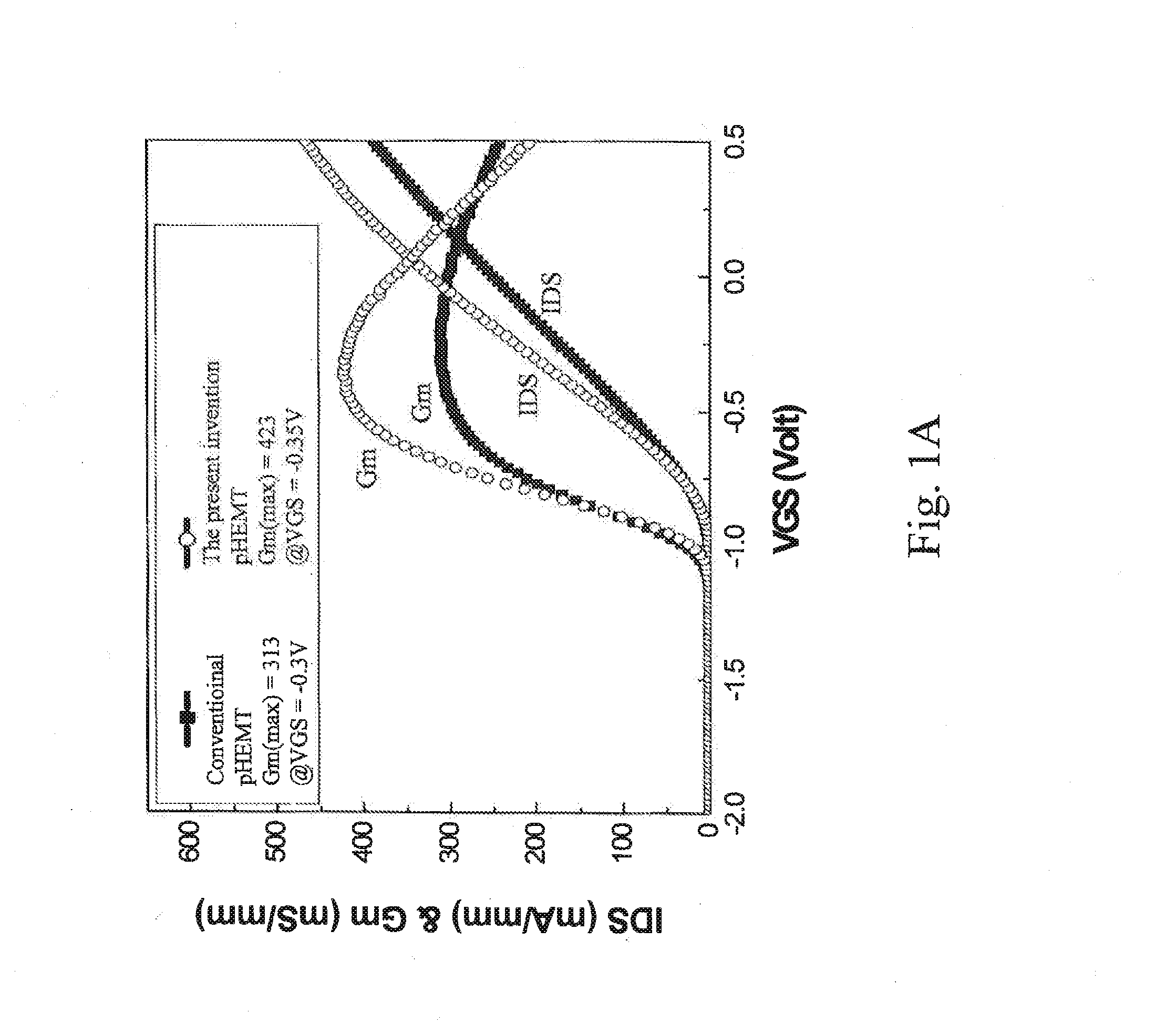
The present invention provides an improved structure for a pHEMT and HBT integrated epitaxial structure. It includes a first and second channel spacer layers to release the compressive strain in the channel layer and reduce the density of defects. The use of two channel spacer layers allows for a desired level of current density, reduced on-resistance, and low insertion loss, as well as stable fabrication process and high device reliability. Additionally, the use of higher Indium content in the channel layer allows for a decrease in resistance but also induces more lattice strain and defects. To address this, a structure is introduced where the first and second channel spacer layers help to release the compressive strain and further reduce the density of defects.

Problems solved by technology

However, higher Indium content will generate higher lattice strain and induce more lattice dislocations and defects.
The lattice dislocations and defects as the traps of electrons will decrease the current density and minimize the advantage of increasing higher Indium content of InGaAs channel layer, or even degrade its original performance.

Method used


Image

  • pHEMT and HBT integrated epitaxial structure
  • pHEMT and HBT integrated epitaxial structure
  • pHEMT and HBT integrated epitaxial structure

Examples


Embodiment Construction

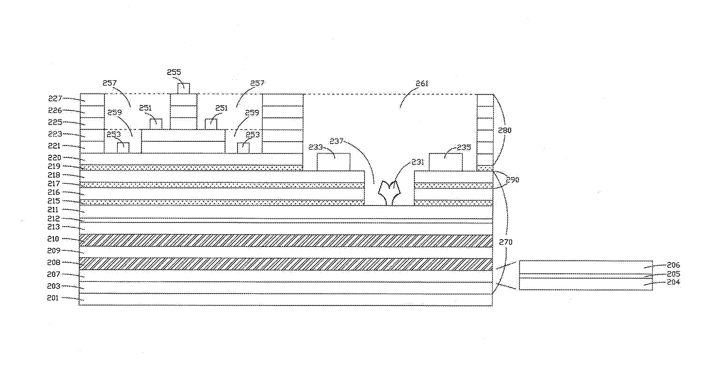
[0040]FIG. 2 is a sectional view of an embodiment of the improved pHEMT epitaxial structure in the present invention, which comprises a substrate 201, a buffer layer 203, a bottom barrier layer 207, a first channel spacer layer 208, a channel layer 209, a second channel spacer layer 210, a Schottky spacer layer 213, a Schottky donor layer 212, a Schottky barrier layer 211, an etching-stop layer 215, at least one cap layer 216, a gate electrode 231, a drain electrode 233, a source electrode 235, and a gate recess 237.

[0041]The substrate 201 is preferably a semi-insulating GaAs substrate. The buffer layer 203 is formed on the substrate 201. The buffer layer 203 can be made of AlGaAs or GaAs, and preferably a combination of an undoped AlGaAs layer and an undoped GaAs layer. The bottom barrier layer 207 is formed on the buffer layer 203. The bottom barrier layer 207 can be made of AlGaAs, and preferably a combination of plural undoped AlGaAs layers and n-type doped AlGaAs layers. The fi...


PUM


Abstract

An improved pseudomorphic high electron mobility transistor (pHEMT) and heterojunction bipolar transistor (HBT) integrated epitaxial structure, in which the structure comprises a substrate, a pHEMT structure, an etching-stop spacer layer, and an HBT structure. The pHEMT structure comprises a buffer layer, a bottom barrier layer, a first channel spacer layer, a channel layer, a second channel spacer layer, a Schottky spacer layer, a Schottky donor layer, a Schottky barrier layer, an etching-stop layer, and at least one cap layer. By introducing the first channel spacer layer and the second channel spacer layer to reduce the density of the dislocations and to reduce the compressive strain in the pseudomorphic channel layer.

Description

CROSS-REFERENCE TO RELATED APPLICATIONS[0001]This application is a Continuation-in-Part of co-pending application Ser. No. 13 / 662,162, filed on Oct. 26, 2012, for which priority is claimed under 35 U.S.C. §120; and this application claims priority of Application No. 101119726 filed in Taiwan, R.O.C. on Jun. 1, 2012 under 35 U.S.C. §119, the entire contents of all of which are hereby incorporated by reference.FIELD OF THE INVENTION[0002]The present invention relates to an improved pseudomorphic high electron mobility transistor (pHEMT) and heterojunction bipolar transistor (HBT) integrated epitaxial structure, in particular to an improved pHEMT and HBT integrated epitaxial structure, in which a first and a second channel spacer layers are included above and below a channel layer respectively.BACKGROUND OF THE INVENTION[0003]Pseudomorphic high electron mobility transistor (pHEMT) and heterojunction bipolar transistor (HBT) have the advantage of high efficiency, high linearity, high po...

Claims


Application Information

Patent Timeline
Patent Type & Authority Applications(United States)
IPC IPC(8): H01L29/778H01L27/06
CPCH01L27/0623H01L29/7782H01L29/66318H01L29/66462H01L29/7371H01L29/7783H01L29/0817H01L29/205H01L21/8252H01L27/0605
Inventor TSAI, SHU-HSIAOLIN, CHENG-KUOHONG, BING-SHANTAKATANI, SHINICHIRO
Owner WIN SEMICON
Learn More