3D NAND flash memory

a memory device and 3d technology, applied in the direction of basic electric elements, semiconductor devices, electrical equipment, etc., can solve the problems of limiting the number of control gates that can be layered in this way, high manufacturing cost, and limiting the use of technology, so as to achieve the effect of higher conductivity

Active Publication Date: 2014-08-21
MACRONIX INT CO LTD
View PDF2 Cites 95 Cited by
  • Summary
  • Abstract
  • Description
  • Claims
  • Application Information

AI Technical Summary

Benefits of technology

[0012]In one aspect of the technology described herein, a reference conductor is disposed between the bottom plane of conductive strips and the substrate. At least one reference line structure is arranged orthogonally over the plurality of stacks, including inter-stack vertical conductive elements between the stacks in electrical communication with the reference conductor. The at least one reference line structure also includes linking elements over the stacks connecting the inter-stack vertical conductive elements. The inter-stack vertical conductive elements can have a higher conductivity than the inter-stack semiconductor body elements.

Problems solved by technology

So, although the benefits of higher density are achieved using three-dimensional (3D) arrays, the higher manufacturing costs limit the use of the technology.
Also, there is a limit in the number of control gates that can be layered in this way, determined by such factors as the conductivity of the vertical channel, program and erase processes that are used and so on.

Method used


Image

  • 3D NAND flash memory
  • 3D NAND flash memory
  • 3D NAND flash memory

Examples


Embodiment Construction

[0029]A detailed description of embodiments of the present invention is provided with reference to the FIGS. 1-33.

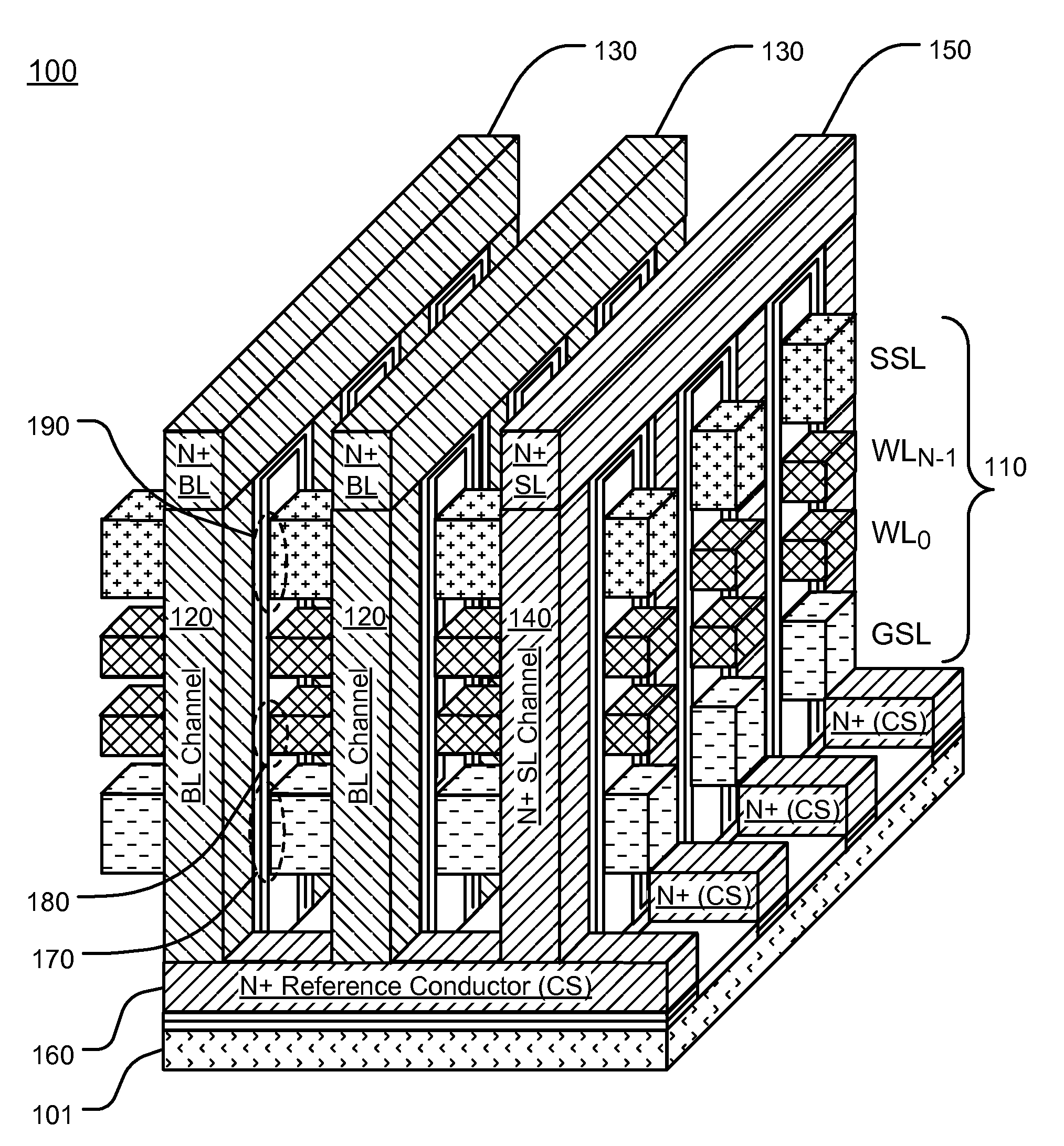
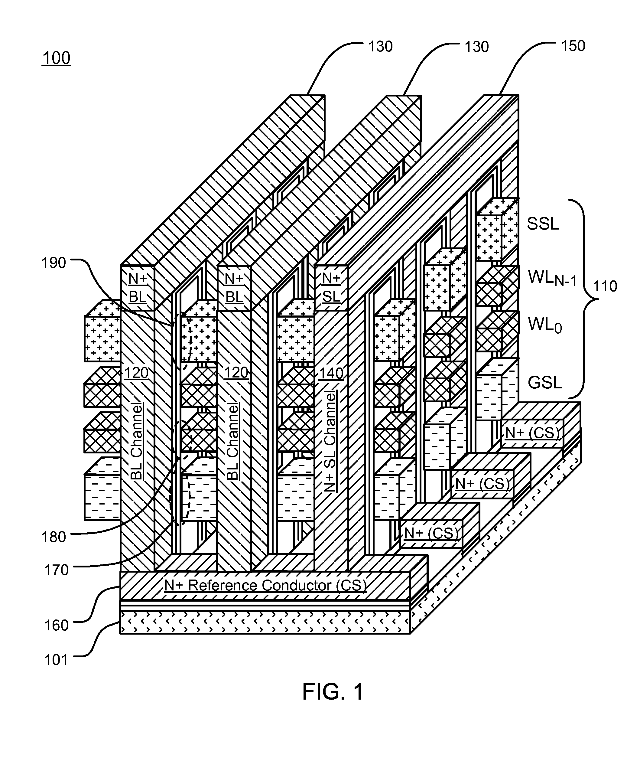
[0030]FIG. 1 is a schematic diagram of a three-dimensional (3D) memory device 100. The memory device 100 includes an array of NAND strings of memory cells, and can be a double-gate vertical channel memory array (DGVC). The memory device 100 includes an integrated circuit substrate, and a plurality of stacks of conductive strips separated by insulating material, including at least a bottom plane of conductive strips (GSL), a plurality of intermediate planes of conductive strips (WLs), and a top plane of conductive strips (SSLs). In the example shown in FIG. 1, a stack 110 includes a bottom plane of conductive strips (GSL), a plurality of intermediate planes of conductive strips (WLs) ranging from WL0 to WLN-1, and a top plane of conductive strips (SSLs), where N can be 8, 16, 32, 64 and so on.

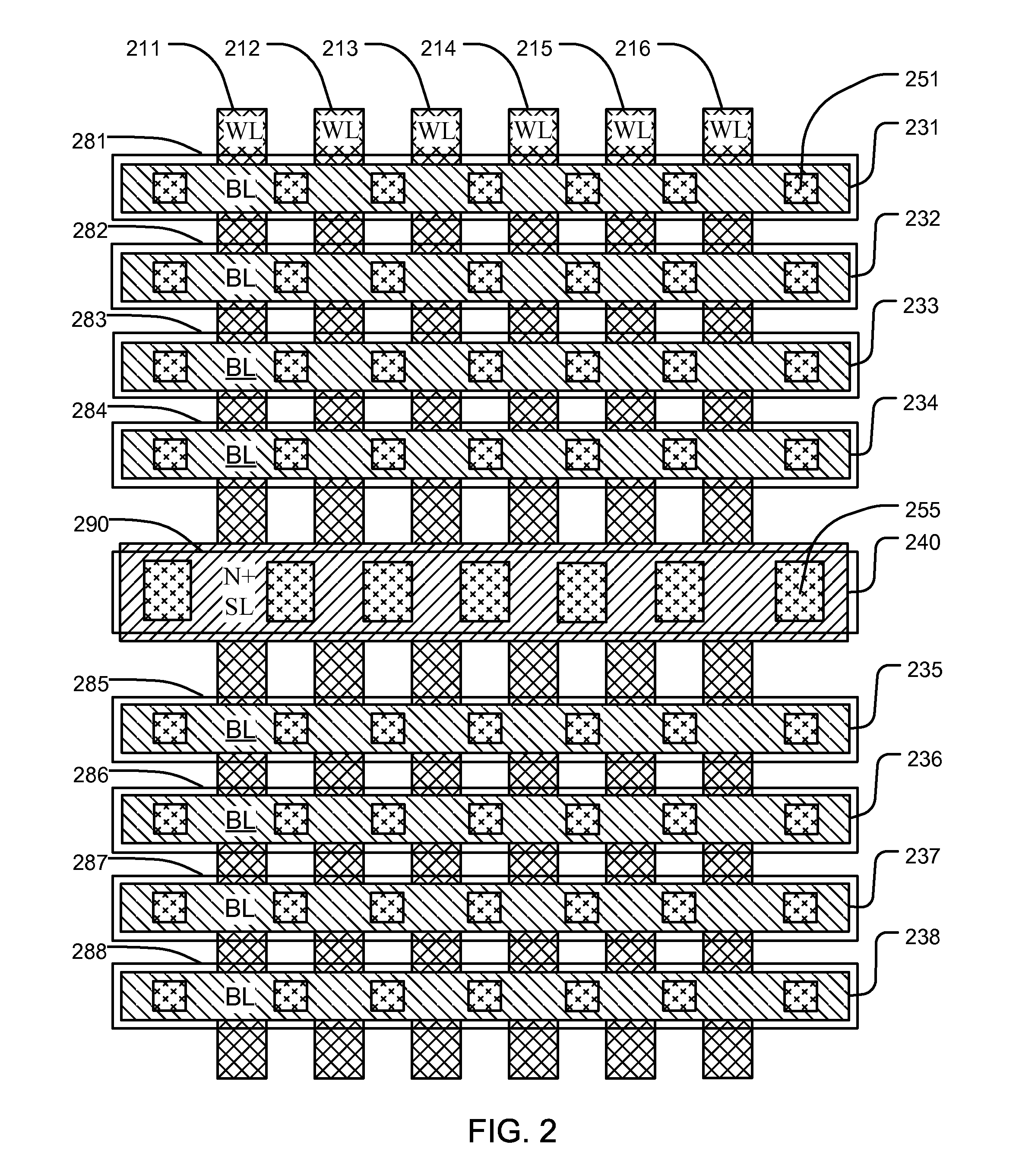
[0031]The plurality of bit line structures are arranged orthogonally over, and h...


PUM

PropertyMeasurementUnit
energyaaaaaaaaaa
semiconductoraaaaaaaaaa
conductivityaaaaaaaaaa

Abstract

A memory device includes an array of NAND strings of memory cells. The device includes a plurality of stacks of conductive strips separated by insulating material, including at least a bottom plane of conductive strips, a plurality of intermediate planes of conductive strips, and a top plane of conductive strips. The device includes charge storage structures in interface regions at cross-points between side surfaces of the conductive strips in the plurality of intermediate planes in the stacks and inter-stack semiconductor body elements of a plurality of bit line structures. At least one reference line structure is arranged orthogonally over the stacks, including vertical conductive elements between the stacks in electrical communication with a reference conductor between the bottom plane of conductive strips and a substrate, and linking elements over the stacks connecting the vertical conductive elements. The vertical conductive elements have a higher conductivity than the semiconductor body elements.

Description

BACKGROUND OF THE INVENTION[0001]1. Field of the Invention[0002]The present invention relates to high density memory devices, and particularly to memory devices in which multiple planes of memory cells are arranged to provide a three-dimensional 3D array.[0003]2. Description of Related Art[0004]As critical dimensions of devices in integrated circuits shrink to the limits of common memory cell technologies, designers have been looking to techniques for stacking multiple planes of memory cells to achieve greater storage capacity, and to achieve lower costs per bit. For example, thin film transistor techniques are applied to charge trapping memory technologies in Lai, et al., “A Multi-Layer Stackable Thin-Film Transistor (TFT) NAND-Type Flash Memory,” IEEE Int'l Electron Devices Meeting, 11-13 Dec. 2006; and in Jung et al., “Three Dimensionally Stacked NAND Flash Memory Technology Using Stacking Single Crystal Si Layers on ILD and TANOS Structure for Beyond 30 nm Node,” IEEE Int'l Elec...

Claims


Application Information

Patent Timeline
Patent Type & Authority Applications(United States)
IPC IPC(8): H01L27/105
CPCH01L27/1052H01L29/7923H10B43/35H10B43/27H10B41/35H10B41/27
Inventor LUE, HANG-TING
Owner MACRONIX INT CO LTD
Why Eureka
Try Eureka