Conductive film and touch panel

a technology which is applied in the field of conductive film and touch panel, can solve the problems of inability to recognize the light transmittance of the conductive film is deteriorated, and the address associated with the broken wire cannot be known, so as to improve the detection sensitivity of touch position, improve the output dynamic range, and improve the light transmittance and visibility

Inactive Publication Date: 2014-08-21
FUJIFILM CORP
View PDF4 Cites 16 Cited by
  • Summary
  • Abstract
  • Description
  • Claims
  • Application Information

AI Technical Summary

Benefits of technology

[0030]As described above, the conductive film and the touch panel of the present invention are excellent in terms of light transmittance and visibil

Problems solved by technology

However, a line width, which is suitable for practical use, is not known from the above documents.
Further, on the condition that one of the thin metal wires is broken, a disadvantage occurs in that the address associated with the broken wire cannot be recognized.
However, in this case, the light transmittance of the conductive film is deteriorated, the touch panel that uses the conductive film exhibits low display brightness,

Method used


Image

  • Conductive film and touch panel
  • Conductive film and touch panel
  • Conductive film and touch panel

Examples


examples

[0183]Examples of the present invention will be described more specifically below. Materials, amounts, ratios, treatment contents, treatment procedures, and the like, which are used in examples, may be appropriately changed without departing from the essential scope of the present invention. Therefore, the following specific examples should be considered in all respects as illustrative and not restrictive.

[0184]In the conductive film stacks 10 of Examples 1 to 8 and Reference Examples 1 and 2, surface resistance and transmittance were measured, and the presence of moiré patterns and visibility were evaluated. The properties, measurement results, and evaluation results of Examples 1 to 8 and Reference Examples 1 and 2 are shown below in Table 3.

examples 1 to 8 and reference examples 1 and 2

Photosensitive Silver Halide Material

[0185]An emulsion containing an aqueous medium, gelatin, and silver iodobromochloride particles was prepared. The amount of gelatin was 10.0 g per 150 g of Ag, and the silver iodobromochloride particles had an I content of 0.2 mol %, a Br content of 40 mol %, and an average spherical equivalent diameter of 0.1 μm.

[0186]K3Rh2Br9 and K2IrCl6 were added to the emulsion at a concentration of 10−7 (mol / mol-Ag) in order to dope the silver bromide particles with Rh and Ir ions. Na2PdCl4 was further added to the emulsion, and the resultant emulsion was subjected to gold-sulfur sensitization using chlorauric acid and sodium thiosulfate. Thereafter, the emulsion and a gelatin hardening agent were applied to each of the first transparent substrate 12A and the second transparent substrate 12B, which were composed of polyethylene terephthalate (PET), such that the amount of applied silver was 10 g / m2 and the Ag / gelatin volume ratio was 2 / 1.

[0187]The PET suppo...

example 1

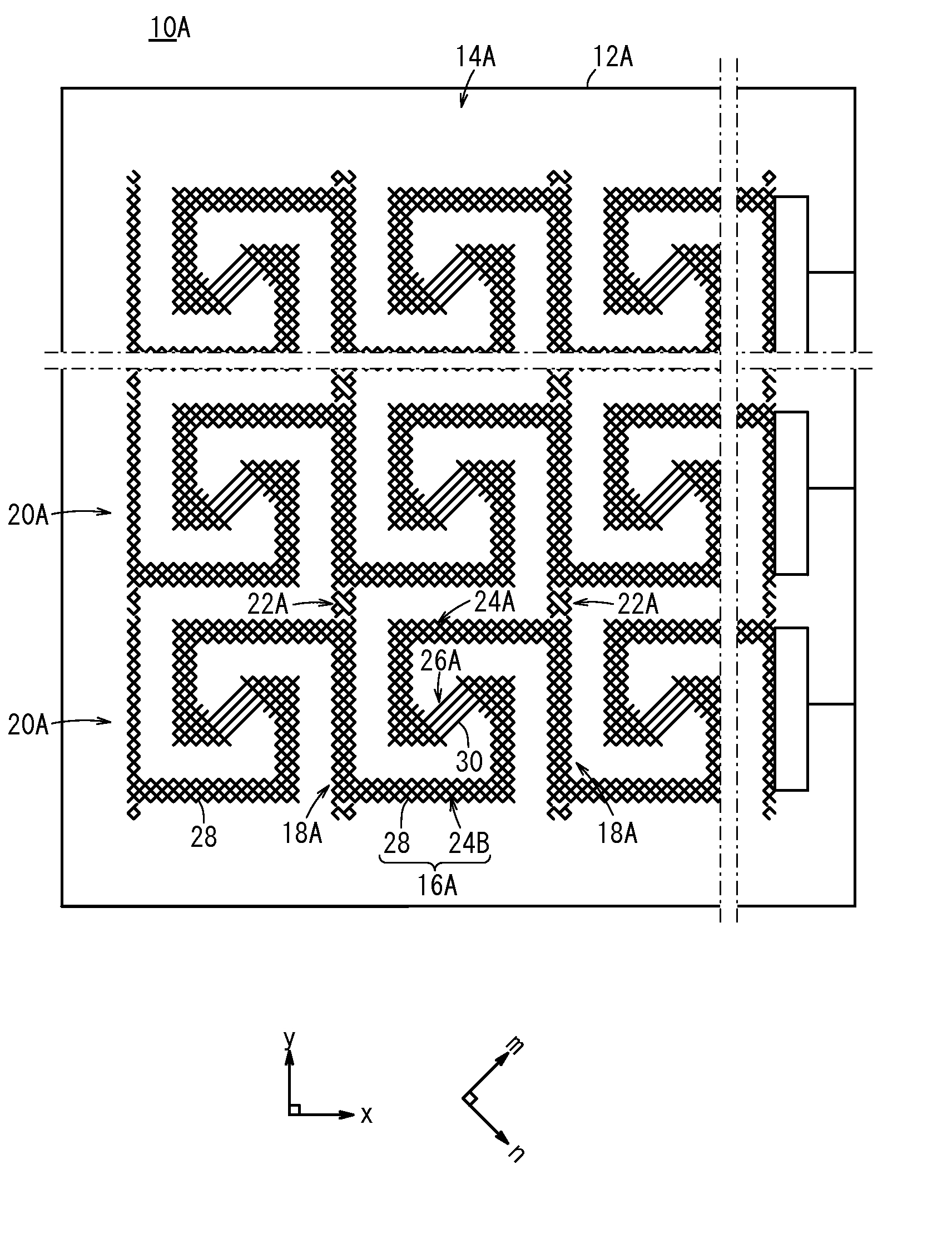
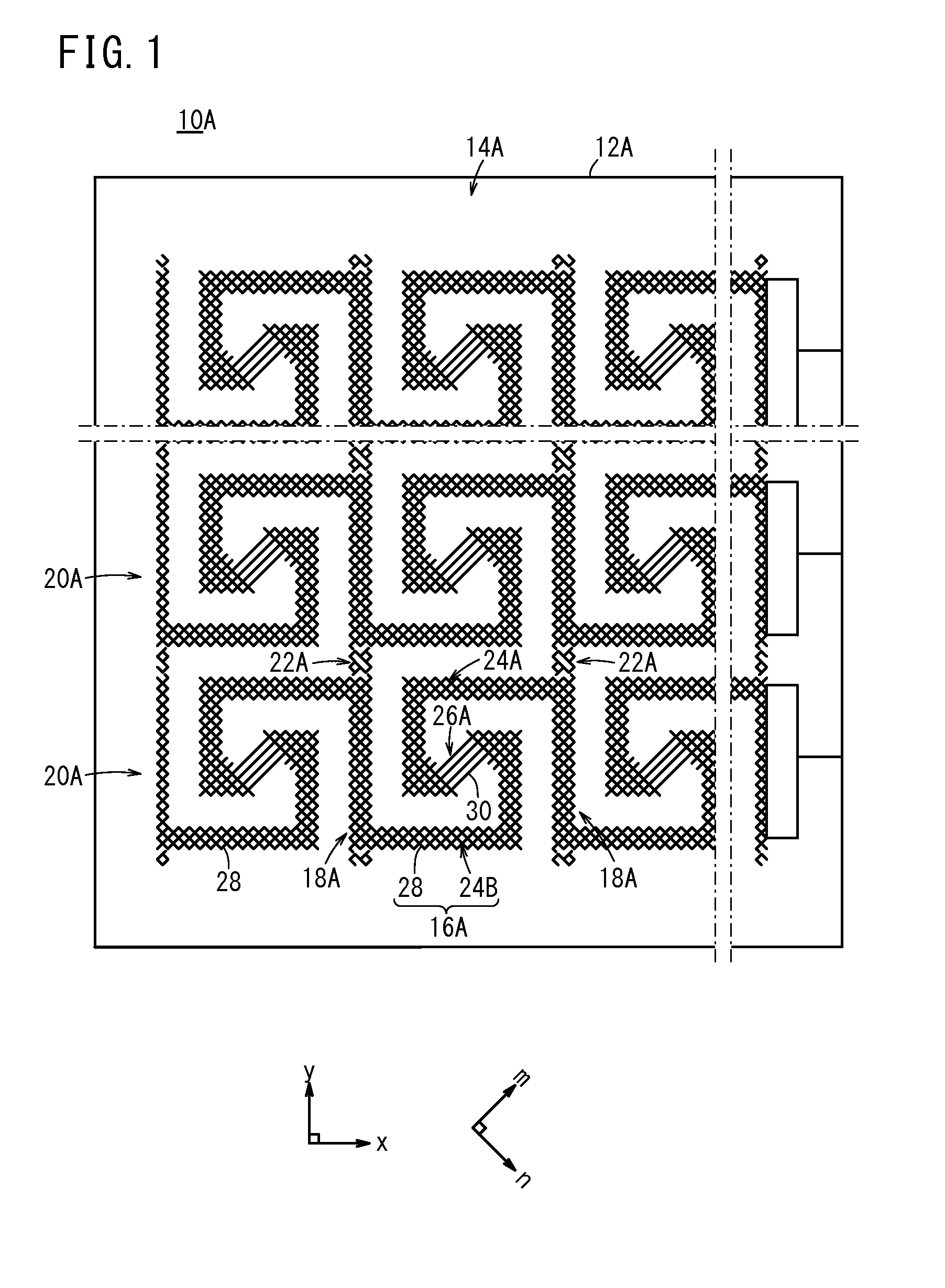
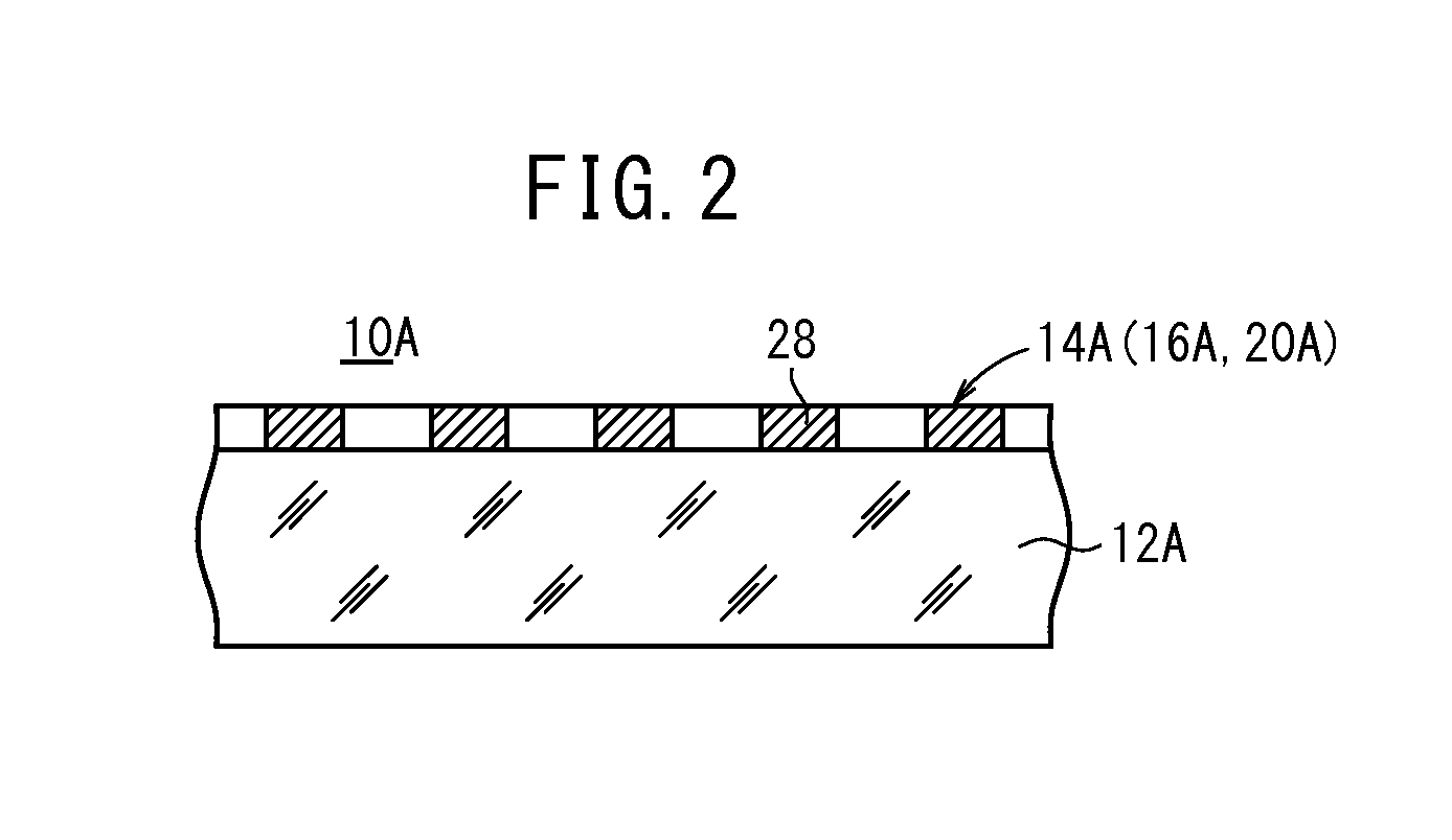
[0192]In the conductive parts (containing the first conductive patterns 20A and the second conductive patterns 20B) of the produced first conductive film 10A and second conductive film 10B, the line width was 1 μm, the side length of the lattice 28 was 100 μm, and the side length of the pad portion (the first pad portion 16A or the second pad portion 16B) was 3 mm.


PUM


Abstract

A first conductive unit of a first conductive film has two or more first conductive patterns made from fine metal wires and including multiple first pads connected through a first connection part. The first pad units are provided with a first spiral unit which extends from one of the first connection units, a second spiral unit which extends from the other first connection unit, and a first connection unit which connects the first spiral unit and the second spiral unit. The first spiral unit and the second spiral unit are configured such that the grids thereof combine, and the first connection unit is configured from multiple conducting wires.

Description

CROSS-REFERENCE TO RELATED APPLICATIONS AND PRIORITY CLAIM[0001]This application is a Continuation of International Application No. PCT / JP2012 / 077589 filed on Oct. 25, 2012, which was published under PCT Article 21(2) in Japanese, which is based upon and claims the benefit of priority from Japanese Patent Application No. 2011-235997 filed on Oct. 27, 2011, the contents all of which are incorporated herein by reference.TECHNICAL FIELD[0002]The present invention relates to a conductive film and a touch panel having a conductive film.BACKGROUND ART[0003]Touch panels have been used mainly in small devices such as PDAs (personal digital assistants) and mobile phones, and are expected to be used in large devices such as personal computer displays.[0004]A conventional electrode for a touch panel is composed of ITO (indium tin oxide) and therefore has a high resistance. Thus, according to the above future trend, on the condition that the conventional electrode is used in a large device, the...

Claims


Application Information

Patent Timeline
IPC IPC(8): G06F1/16H05K1/02
CPCH05K1/02G06F1/1692G06F3/0445G06F3/0446G06F2203/04111G06F2203/04112
Inventor KURIKI, TADASHI
Owner FUJIFILM CORP
Why Eureka
Try Eureka