Optical modulator module and modulation method for optical signal

a technology which is applied in the field of optical modulator module and modulation method of optical signal, can solve the problems of inability to achieve further improvement of transmission distance and transmission speed, inability to respect the modulator region as a uniform distribution any more, and inability to extend the modulator region from a viewpoint of modulation bandwidth improvement, etc., to achieve less distortion

Active Publication Date: 2014-08-21
NEC CORP
View PDF2 Cites 34 Cited by
  • Summary
  • Abstract
  • Description
  • Claims
  • Application Information

AI Technical Summary

Benefits of technology

[0044]The present invention brings an effect that a broadband and low-driving-voltage optical modulator modul

Problems solved by technology

However, when the modulator region length is increased to a degree same as that of the transmission wavelength of a modulation electric signal, a driving electric signal distribution along an optical signal propagation axis with respect to the modulator region cannot be regarded as a uniform distribution any more.
Further, the capacitance of the modulator region increases as it gets longer, and thus, lengthening the modulator region is not acceptable from a viewpoint of a modulation bandwidth improvement.
For this reason, it is deemed to be difficult to achieve further improvements of a transmission distance and a transmission speed by using the binary digital optical intensity modulation method.
Additionally, it is difficult to realize a DAC capable of realizing a response speed of several gigahertz and outputting a voltage higher than or equal to 1 V. Further, in order to obtain a voltage amplitude enough to drive a multi-level modulator (normally around 3.3 to 7 V), it is necessary to provide a driving circuit which amplifies an analog electric signal outputted from a DAC linearly, that is, with least dis

Method used


Image

  • Optical modulator module and modulation method for optical signal
  • Optical modulator module and modulation method for optical signal
  • Optical modulator module and modulation method for optical signal

Examples


first exemplary embodiment

[0071]Hereinafter, exemplary embodiments of the present invention will be described with reference to the drawings.

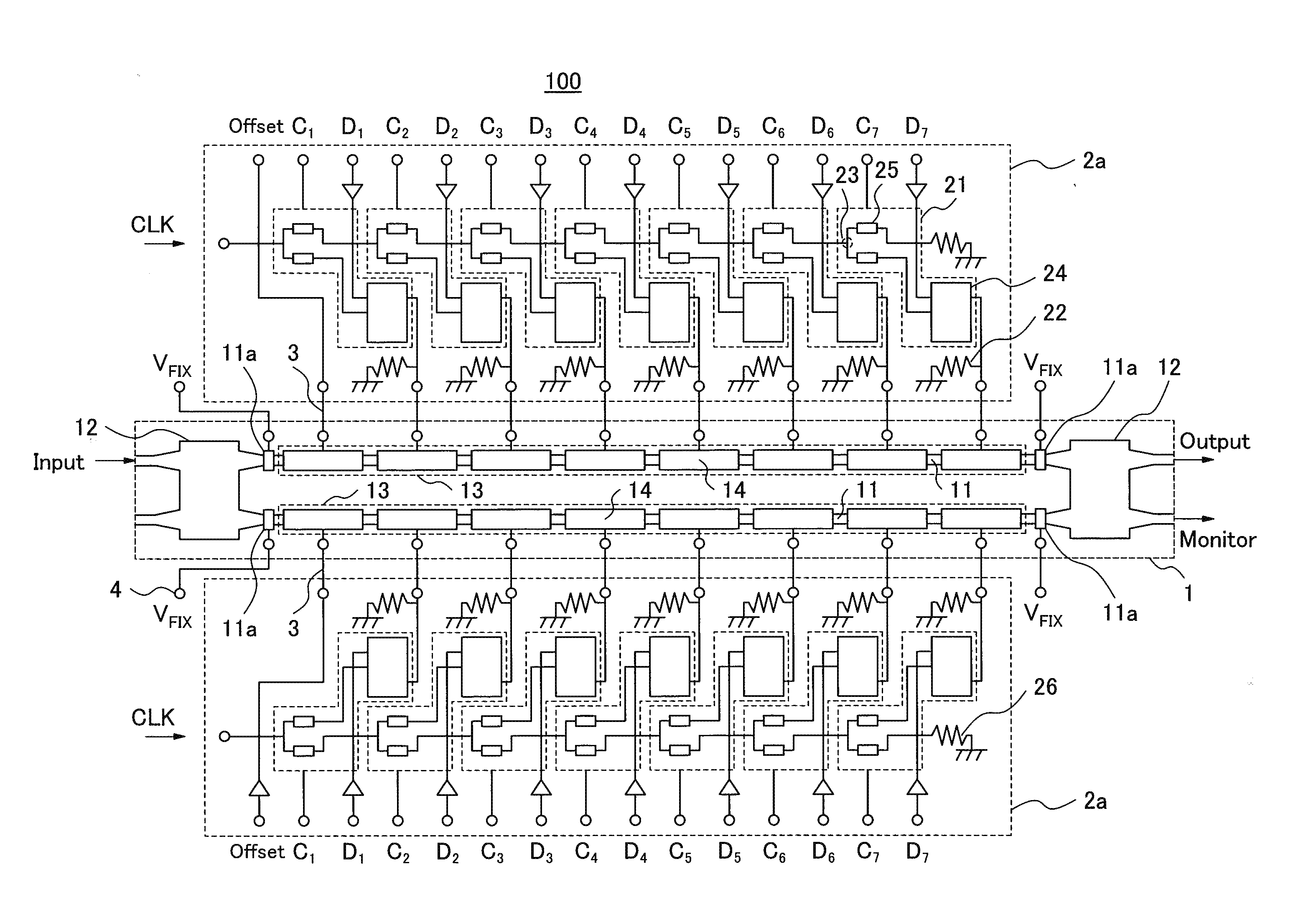
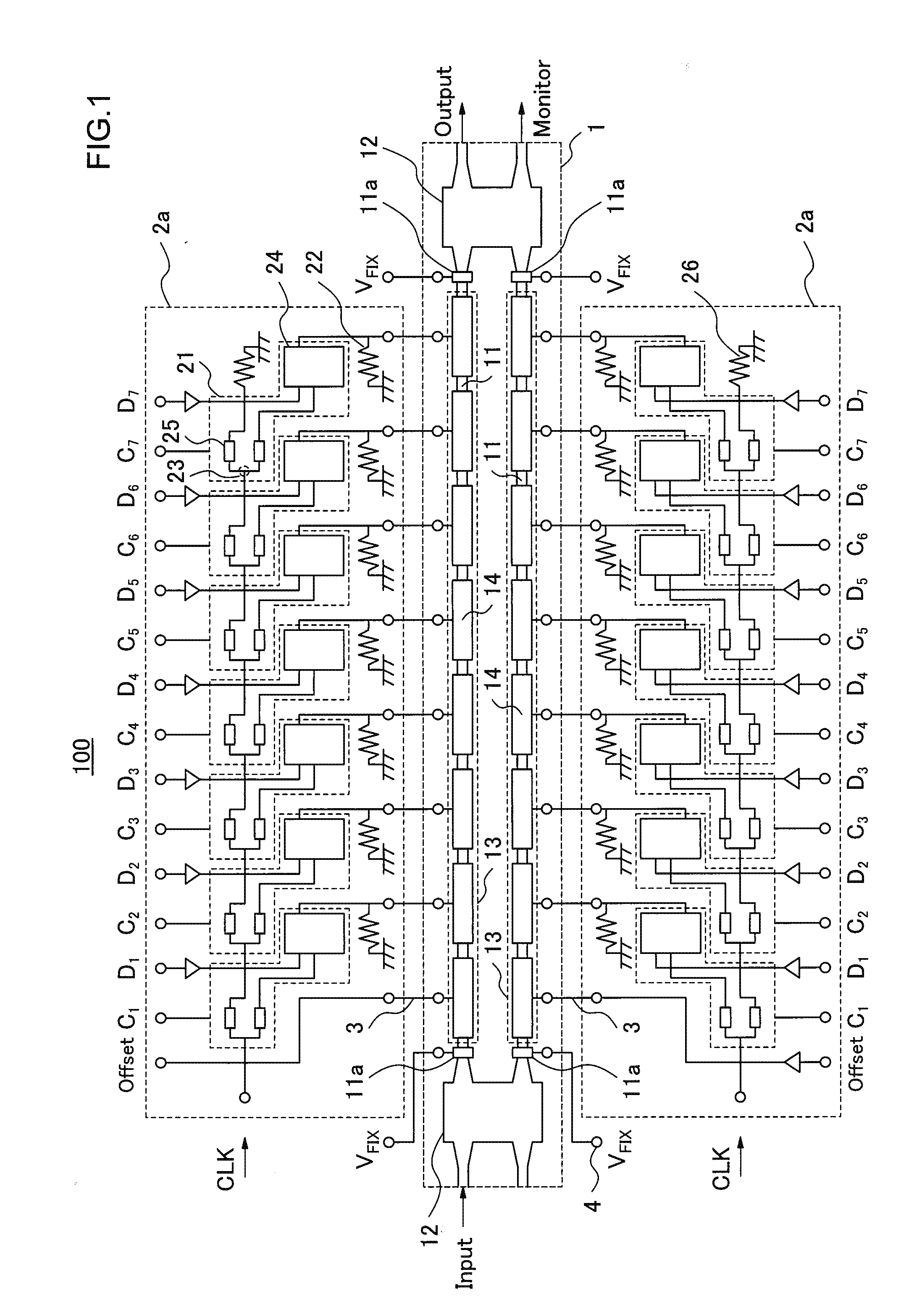
[0072]FIG. 1 is a diagram illustrating a configuration of a multi-level optical modulator module 100 according to a first exemplary embodiment of the present invention. Hereinafter, a configuration of the multi-level optical modulator module 100 will be described. As shown in FIG. 1, the multi-level optical modulator module 100 includes an optical modulator 1 and two integrated circuits 2a.

[0073]The optical modulator 1 includes an MZ interferometer structure provided with two single-mode semiconductor optical waveguides 11 and optical multiplexer / demultiplexer units 12 each having two inputs and two outputs. As shown in FIG. 1, signal light Input is inputted from the left-hand side, and an output signal Output and a monitor output Monitor are outputted from the right-hand side. An optical phase modulator 13 is formed in each of the two semiconductor optical waveguides ...

first example

[0109]A first example is an operation verification example about the multi-level optical modulator module 100 according to the first exemplary embodiment.

[0110]In this example, the semiconductor optical waveguide 11 of the optical modulator 1 is formed on a Fe-doped InP semi-insulating substrate (not illustrated). A core layer and cladding layers which insert the core layer between the cladding layers from upper and lower directions are formed above the Fe-doped InP semi-insulating substrate. The core layer includes an undoped AlGaInAs multiple quantum well layer and undoped InGaAsP light confinement layers which are formed on the upper and lower faces of the undoped AlGaInAs multiple quantum well layer. This configuration is a so-called divided confinement heterostructure (neither of these layers being not illustrated). Here, the configuration of the undoped AlGaInAs multiple quantum well layers is such that: the number of well layers is 12; the thickness of the well layer is 10 nm...

second exemplary embodiment

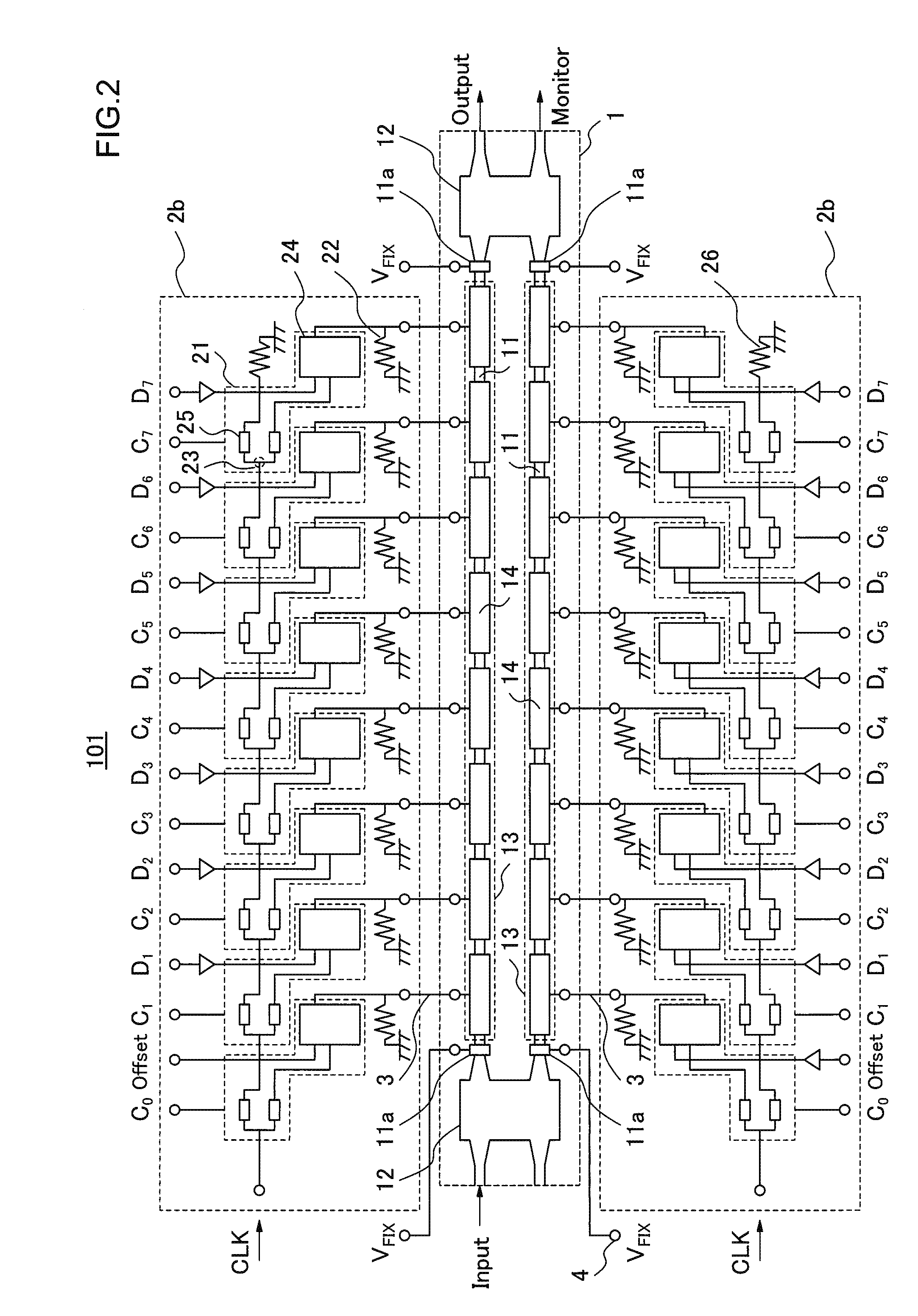
[0115]Next, a programmable multi-level optical modulator module 200 according to a second exemplary embodiment will be described. FIG. 3 is diagram illustrating a configuration of the programmable multi-level optical modulator module 200 according to the second exemplary embodiment. As shown in FIG. 3, in the programmable multi-level optical modulator module 200, the integrated circuit 2a of the multi-level optical modulator module 100 is replaced by an integrated circuit 2c. As compared with the integrated circuit 2a, in the integration circuit 2c, the input interfaces for the digital input signal are changed so that modulator regions targeted for driving can be selected for each group of 2(m−1) stages of the modulator regions.

[0116]A terminal D of a discrete driving circuit connected to the second stage of the modulator regions 14 is supplied with, for example, an offset signal Offset. Further, each of subsequent stages of the modulator regions 14 is supplied with a corresponding ...


PUM


Abstract

An optical modulator module includes an optical modulator including an optical waveguide which conducts an inputted optical signal, and m modulator regions on the optical waveguide; and m discrete driving circuits serially connected to one another. The discrete driving circuits include a driving circuit which outputs a signal obtained from a digital input signal with a synchronization signal to one of the modulator regions, and a phase shifting circuit which outputs a signal resulting from giving a delay to a signal branched from the synchronization signal. A discrete driving circuit receives the signal outputted from the phase shifting circuit. Each of the modulator regions includes modulation electrodes, an electric field caused by a modulation electric signal applied to each of the modulation electrodes penetrates by a penetration length d, and every two adjacent modulation electrodes has a distance Lgap given by Lgap=2d.

Description

TECHNICAL FIELD[0001]The present invention relates to an optical modulator module and a modulation method for an optical signal.BACKGROUND ART[0002]With the explosive growth of demands for broadband multimedia communication services, such as the Internet service and a video streaming service, the introduction of a high-density wavelength multiplexed optical fiber communication system which enables realization of a highly reliable long-distance large-capacity communication system is being promoted in trunk-line systems and metro systems. On the other hand, in subscriber-line systems, optical fiber access services are being rapidly promoted. In these communication systems using optical fibers, a reduction of cost for laying optical fibers which are optical transmission lines and improvement of the transmission band utilization efficiency per optical fiber are important. For this reason, various wavelength multiplexing technologies for transmitting a signal light obtained by multiplexi...

Claims


Application Information

Patent Timeline
IPC IPC(8): H04B10/516
CPCH04B10/516G02F1/025G02F1/0327G02F1/225
Inventor KATO, TOMOAKI
Owner NEC CORP
Why Eureka
Try Eureka