

Photoelectronic device and image sensor
Active Publication Date: 2014-08-28
SAMSUNG ELECTRONICS CO LTD
View PDF22 Cites 18 Cited by
- Summary
- Abstract
- Description
- Claims
- Application Information
AI Technical Summary
Benefits of technology
This patent text describes a device that can capture more light and reduce the flow of electrical current it leaks.
Problems solved by technology
At present, a silicon photodiode is widely used, but typically presents a problem of deteriorated sensitivity, because a silicon photodiode has a smaller absorption area due to smaller pixels.
Method used
View moreImage
Smart ImageViewing Examples

Examples
example 1
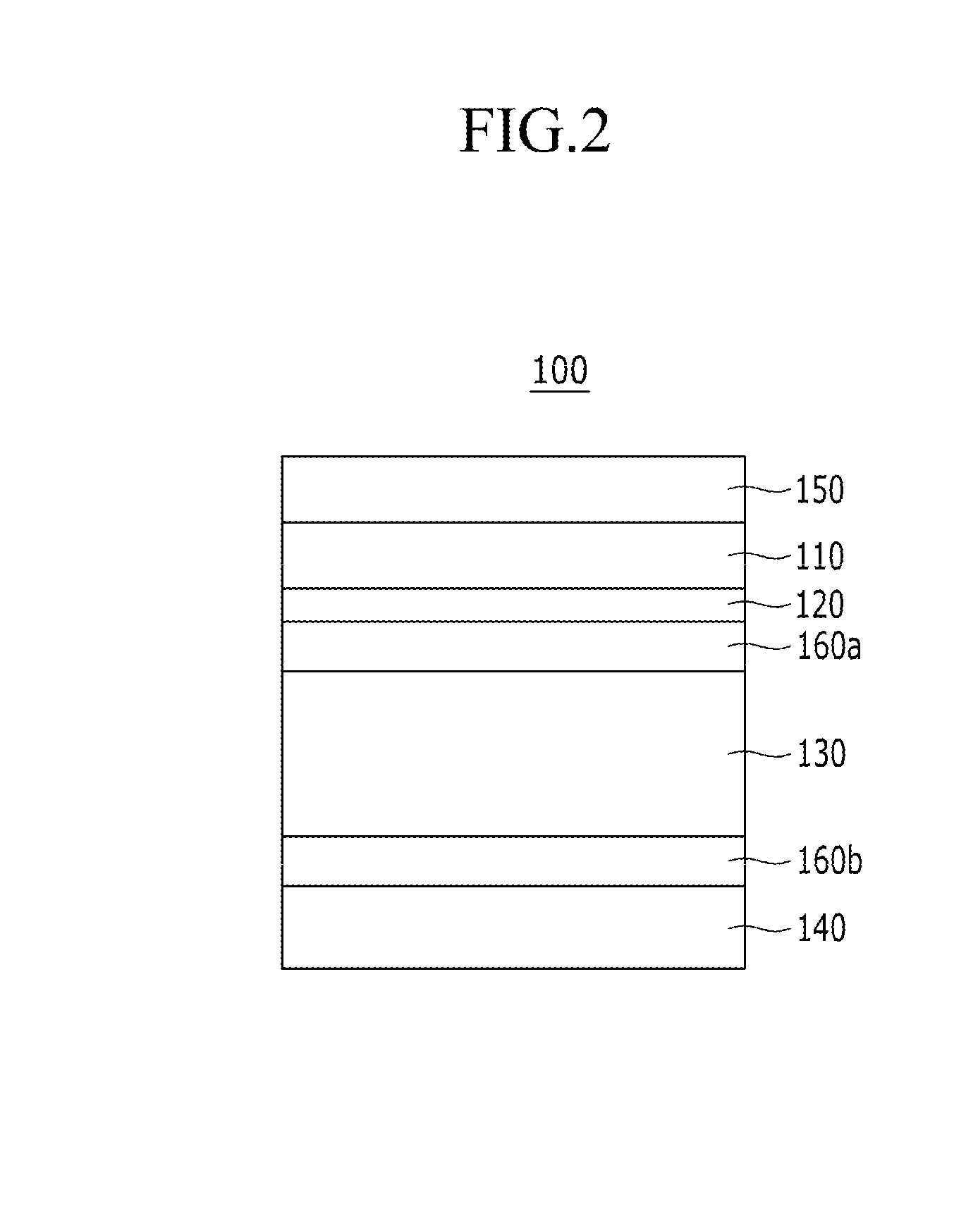
[0096]According to at least one example embodiment, an ITO is sputtered on a glass substrate to form a 100 nm-thick lower electrode. On the lower electrode, a mixture of molybdenum oxide (MoOx, 0−5 m2 / s) is thermally deposited to form a 1 nm-thick diffusion barrier layer, and silver (Ag) (thermal diffusion coefficient: 1.6×10⁻⁴ m2 / s) is thermally deposited to form an 11 nm-thick upper electrode. Then, on the upper electrode, tungsten oxide (WOx, 0<x≦3) is deposited to form a 30 nm-thick light transmission auxiliary layer, fabricating a photoelectronic device.
Login to View More PUM
 Abstract
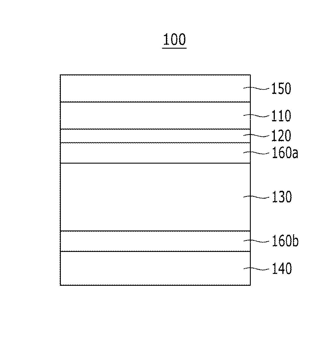
Disclosed are a photoelectronic device including a first electrode including a first metal; an active layer disposed between the first electrode and a second electrode; and a diffusion barrier layer disposed between the first electrode and the active layer; the diffusion barrier layer including a second metal, wherein the second metal has a thermal diffusivity that is lower than a thermal diffusivity of the first metal, and wherein the first electrode and the diffusion barrier layer are configured to transmit light, and an image sensor including the photoelectronic device.
Description
[0001]This application claims priority from Korean Patent Application No. 10-2013-0019422 filed in the Korean Intellectual Property Office on Feb. 22, 2013, the entire contents of which are incorporated herein by reference.BACKGROUNDField[0002]A photoelectronic device and an image sensor are disclosed according to various example embodiments.[0003]A photoelectronic device refers to a device for converting light into an electrical signal. The photoelectronic device may include a photodiode, a phototransistor, and the like, and may be applied to an image sensor, a solar cell, and the like.[0004]In general, an image sensor including a photodiode requires higher resolution and accordingly a smaller pixel. At present, a silicon photodiode is widely used, but typically presents a problem of deteriorated sensitivity, because a silicon photodiode has a smaller absorption area due to smaller pixels. Accordingly, research on an organic materials capable of replacing silicon has been undertake...
Claims
Login to View More Application Information
Patent Timeline
 IPC IPC(8): H01L51/44H01L27/30
CPCH01L51/441H01L27/307H10K39/32H10K30/82Y02E10/549Y02P70/50H01L31/10H01L27/146H01L31/04H10K30/00H10K30/81
InventorPARK, KYUNG BAEKIM, KYU SIKLEE, KWANG HEELEEM, DONG-SEOKLIM, SEON-JEONG
OwnerSAMSUNG ELECTRONICS CO LTD