Semiconductor fin isolation by a well trapping fin portion

a technology of semiconductor fins and well trapping fins, which is applied in the direction of semiconductor devices, basic electric elements, electrical equipment, etc., can solve the problems of additional processing steps, soi substrates are not generally compatible with the use of stress-generating embedded semiconductor materials, and the device formed on a semiconductor fin on a bulk semiconductor substrate suffers from leakage currents

Active Publication Date: 2014-09-11
IBM CORP
View PDF7 Cites 333 Cited by
  • Summary
  • Abstract
  • Description
  • Claims
  • Application Information

AI Technical Summary

Problems solved by technology

Semiconductor devices formed on a semiconductor fin on a bulk semiconductor substrate typically suffer from leakage currents between the semiconductor fin and an underlying semiconductor material of the bulk semiconductor substrate.
While use of a semiconductor-on-insulator (SOI) substrate can provide electrical isolation of semiconductor fins from the substrate, SOI substrates are not generally compatible with use of stress-generating embedded semiconductor materials that can enhance the strain in the channel of a field effect transistor.
Inserting a dielectric material underneath a semiconductor fin requires additional processing steps and increases the total processing time.

Method used


Image

  • Semiconductor fin isolation by a well trapping fin portion
  • Semiconductor fin isolation by a well trapping fin portion
  • Semiconductor fin isolation by a well trapping fin portion

Examples


first embodiment

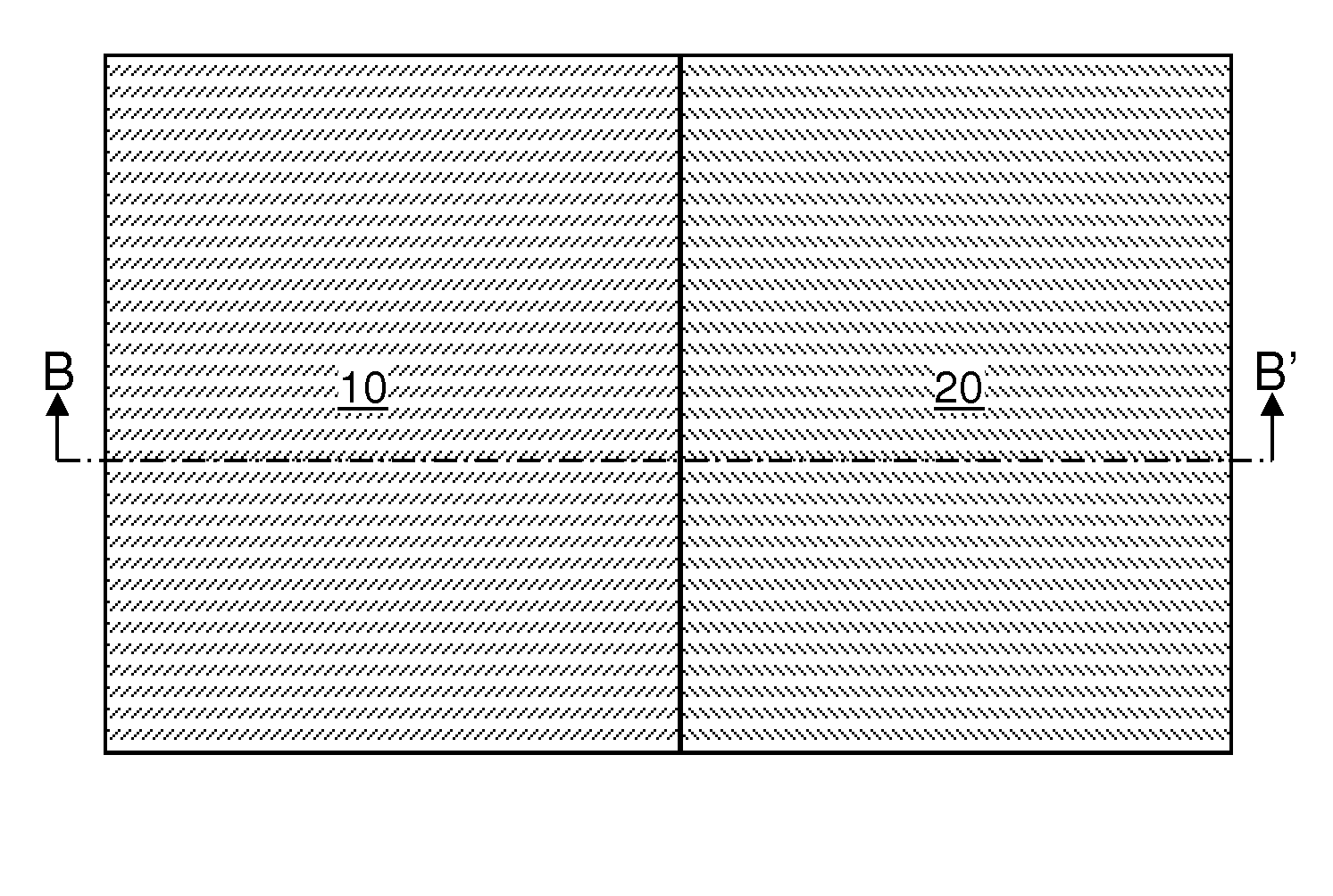
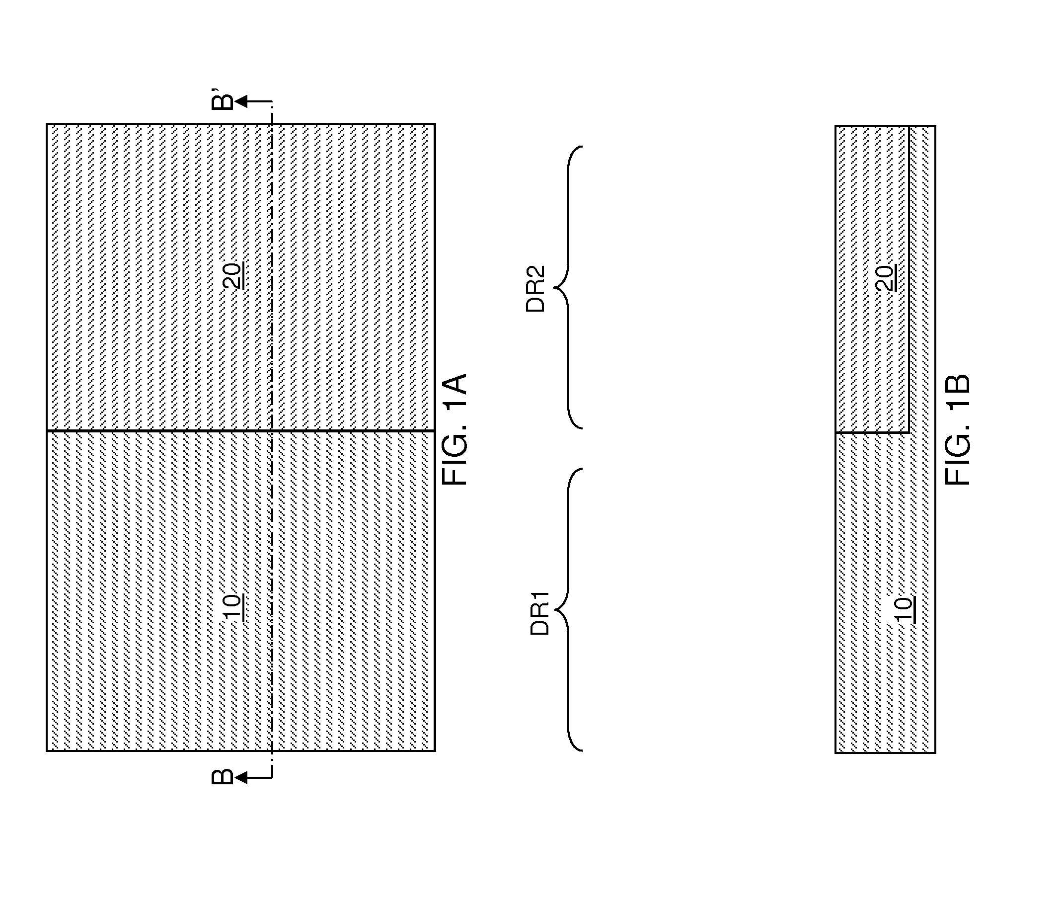
[0051]Referring to FIGS. 1A and 1B, a first exemplary semiconductor structure according to the present disclosure includes a bulk semiconductor substrate including a first semiconductor material throughout. The first semiconductor material can be, for example, single crystalline silicon, a single crystalline silicon-germanium alloy, or a single crystalline silicon-carbon alloy. The bulk semiconductor substrate includes a first semiconductor material layer 10, which can have a p-type doping or an n-type doping. In one embodiment, a doped well 20 can be formed in an upper portion of the bulk semiconductor substrate such that the doped well has a doping of the opposite conductivity type relative to the doping of the first semiconductor material layer. For example, if the first semiconductor material layer 10 has a p-type doping, the doped well 20 has an n-type doping, and vice versa. The doped well 20 is a first semiconductor material portion, i.e., a portion including the first semico...

second embodiment

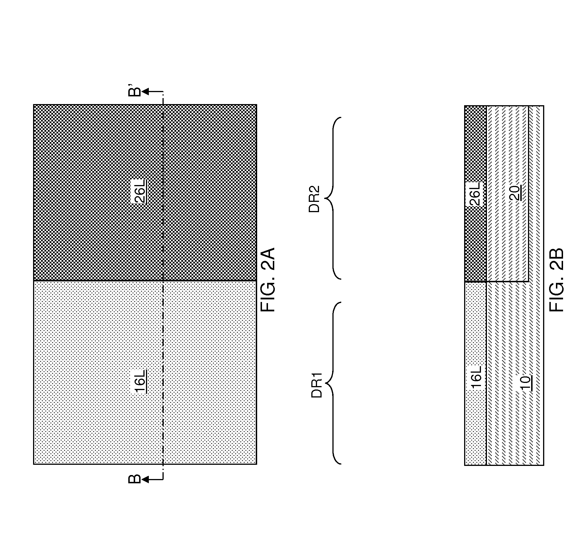
[0093]Non-selective or selective epitaxy can be employed to form the silicon-germanium alloy layer of the In one embodiment, the silicon-germanium alloy layer can be formed as an intrinsic (undoped) single crystalline silicon-germanium alloy layer. The silicon-germanium alloy layer can have an atomic concentration of germanium in a range from 1% to 80%, the atomic concentration of silicon being the balance. The thickness of the silicon-germanium alloy layer 26L can be in a range from 10 nm to 100 nm, although lesser and greater thicknesses can also be employed. The material of the silicon-germanium alloy layer 26L, i.e., the silicon-germanium alloy, is the second semiconductor material for the first device region DR1 and the second device region DR2.

[0094]N-type dopants are introduced into the portion of the silicon-germanium layer in the first device region DR1 employing a masked ion implantation process. P-type dopants are introduced into the portion of the silicon-germanium allo...


PUM

PropertyMeasurementUnit
thicknessesaaaaaaaaaa

Abstract

A bulk semiconductor substrate including a first semiconductor material is provided. A well trapping layer including a second semiconductor material and a dopant is formed on a top surface of the bulk semiconductor substrate. The combination of the second semiconductor material and the dopant within the well trapping layer is selected such that diffusion of the dopant is limited within the well trapping layer. A device semiconductor material layer including a third semiconductor material can be epitaxially grown on the top surface of the well trapping layer. The device semiconductor material layer, the well trapping layer, and an upper portion of the bulk semiconductor substrate are patterned to form at least one semiconductor fin. Semiconductor devices formed in each semiconductor fin can be electrically isolated from the bulk semiconductor substrate by the remaining portions of the well trapping layer.

Description

BACKGROUND[0001]The present disclosure relates to a semiconductor structure, and particularly to semiconductor fins electrically isolated from an underlying semiconductor layer by a well trapping fin portion and a method of manufacturing the same.[0002]Semiconductor devices formed on a semiconductor fin on a bulk semiconductor substrate typically suffer from leakage currents between the semiconductor fin and an underlying semiconductor material of the bulk semiconductor substrate. For example, the source region and the drain region of a fin field effect transistor can have leakage paths to the underlying semiconductor material.[0003]While use of a semiconductor-on-insulator (SOI) substrate can provide electrical isolation of semiconductor fins from the substrate, SOI substrates are not generally compatible with use of stress-generating embedded semiconductor materials that can enhance the strain in the channel of a field effect transistor. Inserting a dielectric material underneath ...

Claims


Application Information

Patent Timeline
Patent Type & Authority Applications(United States)
IPC IPC(8): H01L29/78H01L29/66
CPCH01L29/66795H01L29/785H01L21/823821H01L27/0924H01L27/0886H01L29/0649H01L29/1608H01L29/161H01L29/165H01L29/167H01L29/7849H01L21/823431H01L29/0847H01L29/1095
Inventor UTOMO, HENRY K.CHENG, KANGGUODIVAKARUNI, RAMACHANDRARAMACHANDRAN, RAVIKUMARSHANG, HUILINGVEGA, REINALDO A.
Owner IBM CORP
Why Eureka
Try Eureka