Superlattice crenelated gate field effect transistor

a field effect transistor and super-lattice technology, applied in the direction of transistors, electrical devices, semiconductor devices, etc., can solve the problems of inability to completely “off”, excessively large leakage current, and difficulty in improving (e.g., lowering) insertion loss, and achieve the effect of effectively controlling all 2dxg channels

Active Publication Date: 2014-09-18
NORTHROP GRUMMAN SYST CORP
View PDF5 Cites 32 Cited by
  • Summary
  • Abstract
  • Description
  • Claims
  • Application Information

AI Technical Summary

Benefits of technology

[0014]In general, the present invention is directed to a field-effect transistor device comprising a superlattice structure having a plurality of 2DxG channels therewithin, a source, a

Problems solved by technology

Given the inversely-proportional relationship between on-resistance and off-capacitance, it is difficult to improve (e.g., lower) insertion loss while not adversely impacting (e.g., lowering) the isolation simultaneously.
While the prior art has been able to fabricate, in

Method used


Image

  • Superlattice crenelated gate field effect transistor
  • Superlattice crenelated gate field effect transistor
  • Superlattice crenelated gate field effect transistor

Examples


example 1

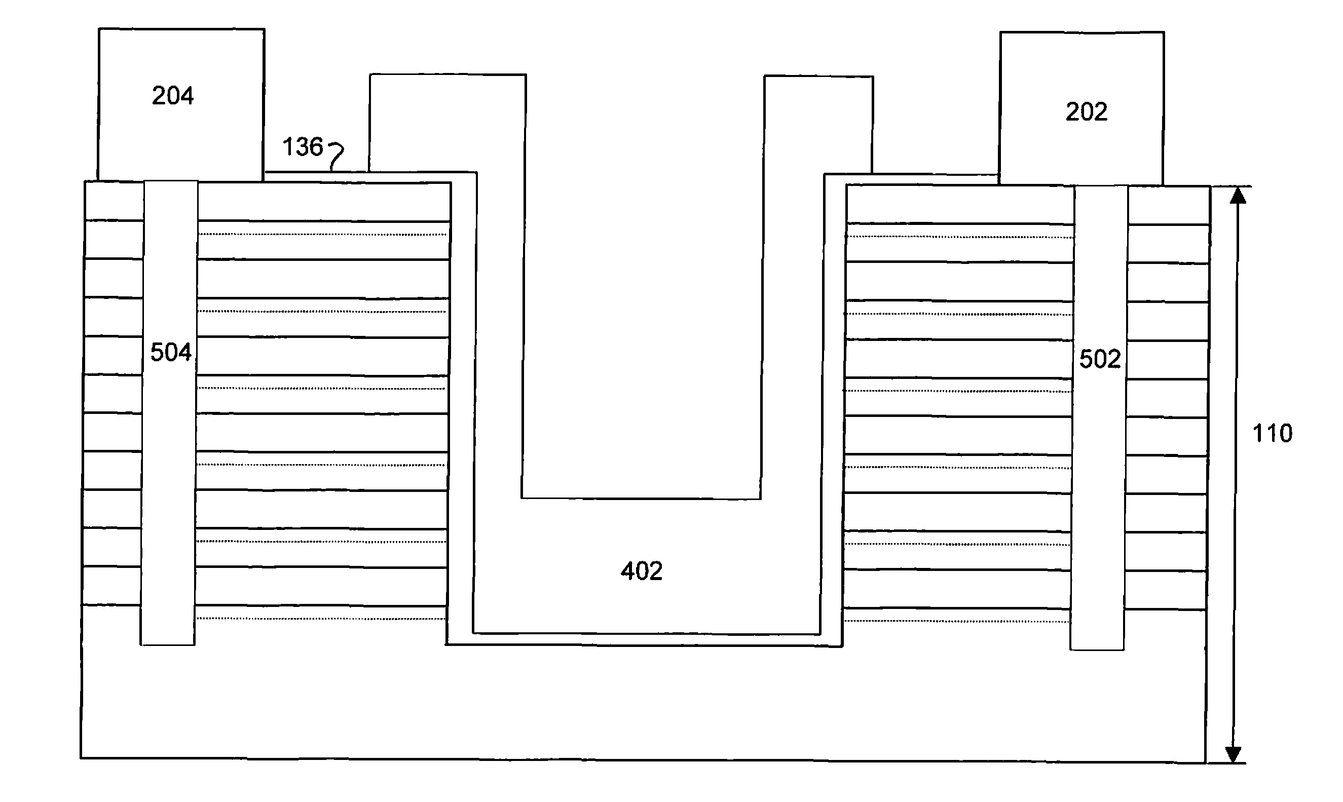
[0051]A normally-on field effect transistor was designed having a source, drain and gate deposited upon an epitaxy having a superlattice structure comprising six heterostructures, each heterostructure containing a 2DEG channel therewithin, each heterostructure formed by a layer of 40% graded AlGaN over a layer of GaN. The six AlGaN layers were each about 7.5 nanometers thick. The top five GaN layers were each about 8 nanometers thick, with the bottommost GaN layer being about 50 nanometers thick. A planar, Schottky gate was deposited thereon between source and drain. Various gate voltages were applied in an effort to determine the effective gate voltage required to turn “off” all 2DEG channels within the device. A gate voltage of −20V was shown to penetrate the superlattice structure to just below the second 2DEG channel, halting current flow through the top two 2DEG channels while allowing current to flow through the other four 2DEG channels therebelow. A gate voltage of −100V was ...

example 2

[0075]A normally-on field effect transistor was designed as described with reference to Example 1, and further comprising about 1000 trenches, each trench having a length of 0.6 microns, a width of 0.05 microns and a depth below all six 2DEG channels, wherein the trenches were spaced 0.08 microns apart from each other. The angle of the trench sidewalls (i.e., angle 302 and angle 304) was about 96 degrees. A gate electrode having a length of about 0.25 microns and a width of about 67 microns was deposited onto the superlattice structure and within each of the trenches such that the bottom portion of the gate electrode was also below all six 2DEG channels. The device had the following characteristics: drain current of 2.68 A / mm at 5 Vd; Ron was 0.49 ohms·mm; and Coff was 0.2 pF / mm. Various gate voltages were applied in an effort to determine the effective gate voltage [Vg] required to turn “off” all 2DEG channels within the device. Several devices were manufactured over time, and each...


PUM


Abstract

The present invention is directed to a device comprising an epitaxial structure comprising a superlattice structure having an uppermost 2DxG channel, a lowermost 2DxG channel and at least one intermediate 2DxG channel located between the uppermost and lowermost 2DxG channels, source and drain electrodes operatively connected to each of the 2DxG channels, and a plurality of trenches located between the source and drain electrodes. Each trench has length, width and depth dimensions defining a first sidewall, a second sidewall and a bottom located therebetween, the bottom of each trench being at or below the lowermost 2DxG channel. A crenelated gate electrode is located over the uppermost 2DxG channel, the gate electrode being located within each of the trenches such that the bottom surface of the gate electrode is in juxtaposition with the first sidewall surface, the bottom surface and the second sidewall surface of each of said trenches.

Description

BACKGROUND OF THE INVENTION[0001]1. Technical Field[0002]The present invention is directed to a heterostructure Field-Effect Transistor (“FET”). More particularly, the present invention is directed to a heterostructure FET having a superlattice structure with a plurality of Two-Dimensional Electron Gas (2DEG) channels, all of which are capable of being turned “off” by the application of a relatively low gate voltage. The present invention is equally applicable to superlattice structures having a plurality of Two-Dimensional Hole Gas (2DHG) channels. The present invention finds particular utility as a normally-on RF switch.[0003]2. Background Information[0004]A high-quality RF switch is ideally designed to minimize the on-resistance, Ron, while also minimizing the off-capacitance, Coff. An ideal RF switch, when “on”, passes a signal without attenuation, distortion or insertion loss (all of which being a function of on-resistance) and, when “off”, isolates the signal and prevents it f...

Claims


Application Information

Patent Timeline
IPC IPC(8): H01L29/778H01L29/15
CPCH01L29/15H01L29/7784H01L29/0843H01L29/0847H01L29/1029H01L29/1037H01L29/2003H01L29/66462H01L29/155H01L29/41766
Inventor HOWELL, ROBERT S.STEWART, ERIC J.NECHAY, BETTINA A.PARKE, JUSTIN A.CRAMER, HARLAN C.HARTMAN, JEFFREY D.
Owner NORTHROP GRUMMAN SYST CORP
Why Eureka
Try Eureka