Method and system for forming a diagonal pattern using charged particle beam lithography

Active Publication Date: 2014-09-18
D2S
View PDF2 Cites 2 Cited by
  • Summary
  • Abstract
  • Description
  • Claims
  • Application Information

AI Technical Summary

Benefits of technology

[0015]A method and system for fracturing or mask data preparation is disclosed in which a middle or central core portion of a diagonal pattern is fractured using overlapping variable shaped beam (VSB) shots, and an outer portion of the diagonal pattern is fractured using non-overlapping VSB shots. A transition region is interposed between the central core portion of the pattern and the outer portion of the pa

Problems solved by technology

An example of an end-use limitation is defining the geometry of a transistor in a way in which it cannot sufficiently operate at the required supply voltage.
The design rule limitations reflect, among other things, the smallest dimensions that can be reliably fabricated.
As the critical dimensions of the circuit pattern become smaller and approach the resolution value of the exposure tool, the accurate transcription of the physical design to the actual circuit pattern developed on the resist layer becomes difficult.
Adding OPC features is a very laborious task, requires costly computation time, and results in more expensive reticles.
Not only are OPC patterns complex,

Method used


Image

  • Method and system for forming a diagonal pattern using charged particle beam lithography
  • Method and system for forming a diagonal pattern using charged particle beam lithography
  • Method and system for forming a diagonal pattern using charged particle beam lithography

Examples


Embodiment Construction

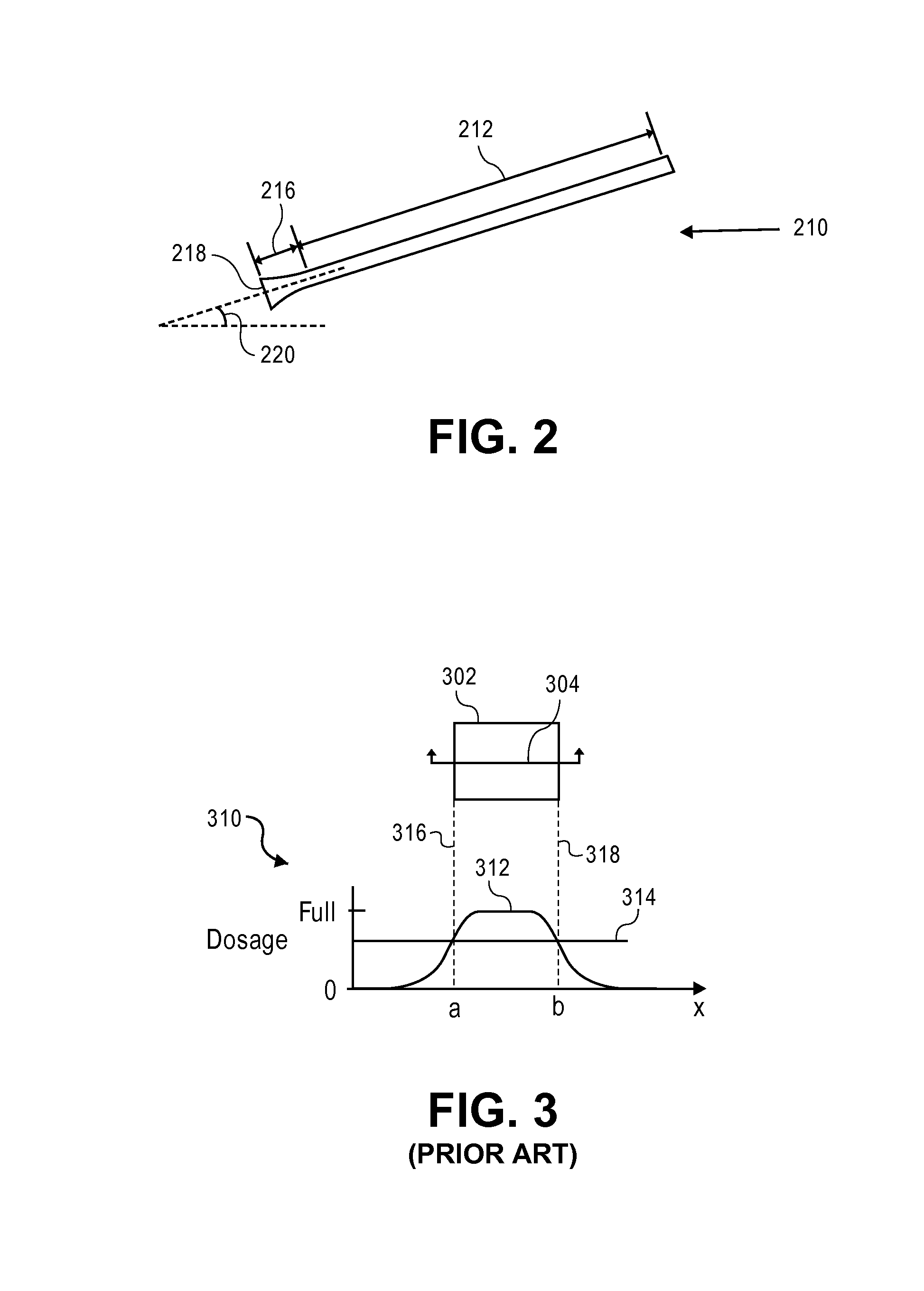
[0043]The improvements and advantages of the present disclosure can be accomplished by forming center portions of continuous track-type patterns using overlapping rectangular variable shaped beam (VSB) shots, by forming near-end portions of the track-type patterns using non-overlapping rectangular VSB shots, and by generating shots for one or more transition regions between the center and near-end portions of the patterns, such that the transition region shots form smooth pattern transitions on the surface of a substrate or wafer between the center and the near-end portions of the patterns.

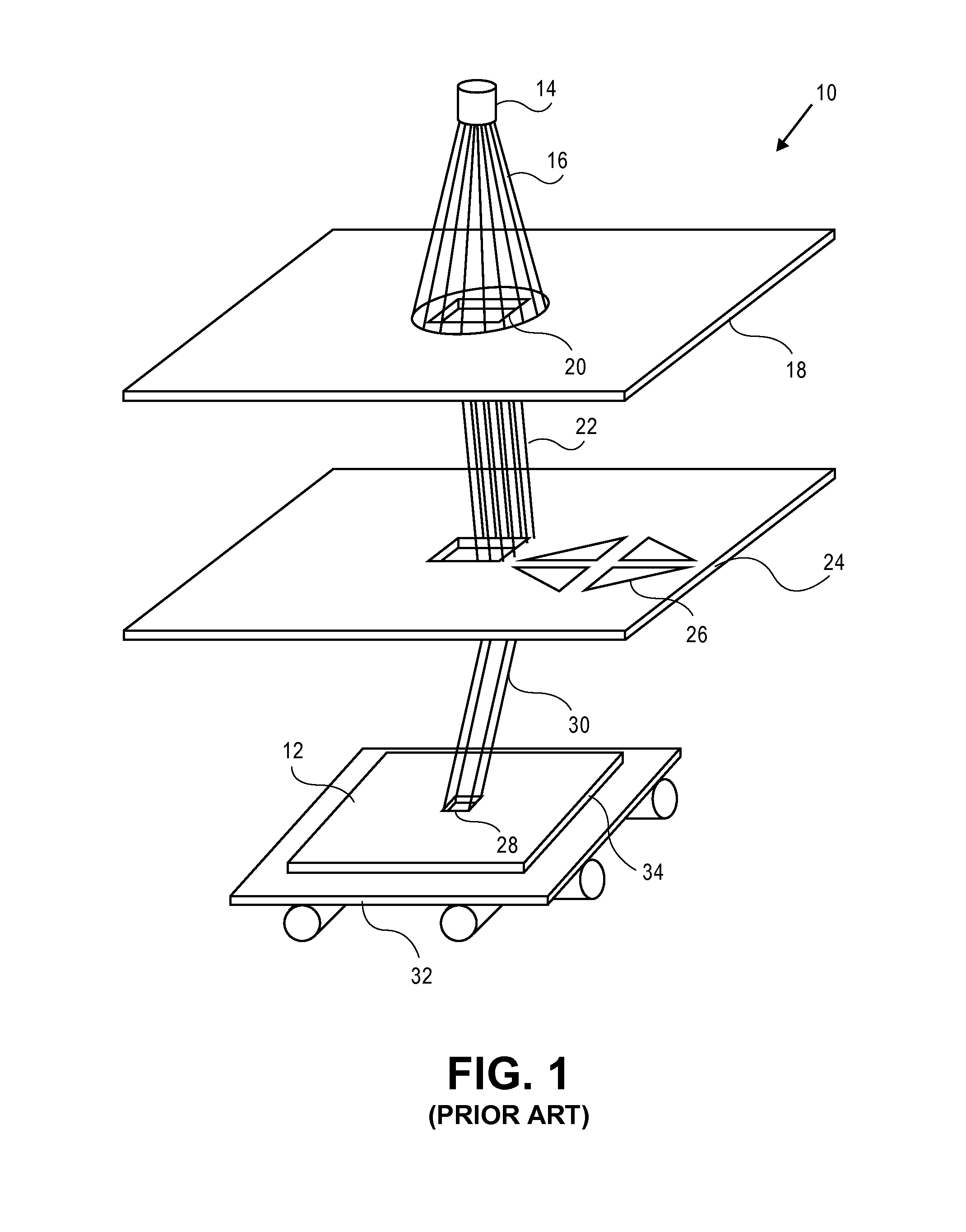
[0044]Referring now to the drawings, wherein like numbers refer to like items, FIG. 1 identifies an embodiment of a lithography system, such as a charged particle beam writer system, in this case an electron beam writer system 10, that employs a variable shaped beam (VSB) to manufacture a surface 12 according to the present disclosure. The electron beam writer system 10 has an electron beam source...


PUM


Abstract

A method and system for fracturing or mask data preparation is disclosed in which the central core portion of a diagonal pattern is fractured using overlapping variable shaped beam (VSB) shots, and an outer portion of the diagonal pattern is fractured using non-overlapping VSB shots. A transition region is interposed between the central core and outer pattern portions, and transition region shots are generated so as to produce in the transferred pattern a smooth transition in pattern characteristics such as line edge roughness or period of waviness, from the central core portion of the pattern to the outer portion of the pattern. A pattern determined by the transition region shots is then compared to a reticle pattern created using conventional non-overlapping VSB shots. Methods for forming a semiconductor device layout pattern on a reticle or substrate are also disclosed.

Description

RELATED APPLICATIONS[0001]This application is related to Jacques, U.S. patent application Ser. No.______ (Attorney Docket D2SiP037a), entitled “Method and System for Forming a Diagonal Pattern Using Charged Particle Beam Lithography”, filed on even date herewith, and hereby incorporated by reference for all purposes.BACKGROUND OF THE DISCLOSURE[0002]The present disclosure is related to lithography, and more particularly to the design and manufacture of a surface which may be a reticle, a wafer, or any other surface, using charged particle beam lithography.[0003]In the production or manufacturing of semiconductor devices, such as integrated circuits, optical lithography may be used to fabricate the semiconductor devices. Optical lithography is a printing process in which a lithographic mask or photomask manufactured from a reticle is used to transfer patterns to a substrate such as a semiconductor or silicon wafer to create the integrated circuit (I.C.). Other substrates could includ...

Claims


Application Information

Patent Timeline
IPC IPC(8): G06F17/50
CPCG06F17/50H01J37/3174H01J2237/31764G03F1/78G06F30/00
Inventor JACQUES, ETIENNECHOI, JINHAGIWARA, KAZUYUKI
Owner D2S
Why Eureka
Try Eureka