Nanostructure, nanostructure fabrication method, and photovoltaic cell incorporating a nanostructure

a nanostructure and photovoltaic cell technology, applied in the field of nanostructures, can solve the problems of degrading optoelectronic properties and unfavorable growth of such nanostructures, and achieve the effects of promoting light reflection, promoting light reflection, and promoting separation of charge carriers

Inactive Publication Date: 2014-09-25
GASP SOLAR APS
View PDF3 Cites 2 Cited by
  • Summary
  • Abstract
  • Description
  • Claims
  • Application Information

AI Technical Summary

Benefits of technology

[0022]In one embodiment of a multi-junction photovoltaic cell, according to the invention, the silicon in the substrate may form a first p-n junction and the GaAsP in the nanostructures forms a second p-n junction. The band gap of the first p-n junction may be different from (e.g. lower than) that of the second p-n junction to enable the cell to generate electricity from a broad range of wavelengths in the light spectrum.
[0023]Herein, a p-n junction may mean any arranged of a first region having a first conductivity type (e.g. p-conductivity) with respect to a second region having a second conductivity type different from (e.g. opposite to) the first conductivity type (e.g. n-conductivity) which promotes separation of charge carriers (i.e. electron-hole pairs) created by the absorption of photons in the first or second region to generate a voltage across the cell. For example, the first and second region may contact one another at an interface, thereby creating a p-n junction. Alternatively, in a preferred arrangement, a substantially intrinsic region may be located between the first and second regions to form a p-i-n junction.
[0024]In one embodiment, the silicon substrate may comprise a first silicon layer having a first conductivity type, and a second silicon layer having a second conductivity type, the first and second silicon layers being disposed to form the first p-n junction (or p-i-n junction), and each GaAsP nanostructure may have a core region surrounded by a shell region, the core region being formed from one of the first and second conductivity types (e.g. n+-doped GaAsP) and the shell region being formed from the other of the first and second conductivity types (e.g. p+-doped GaAsP) to form a second p-n junction (or p-i-n junction if a region (e.g. an inner shell region) of substantially intrinsic GaAsP is disposed between the core and shell regions).
[0025]A third p-n junction (e.g. a tunnel junction) may be provided between the first and second p-n junctions. The third p-n junction is formed in the silicon substrate or in each GaAsP nanostructure or at the interface between the Si substrate and the GaAsP nanostructures.
[0026]As is conventional, a first electrical contact may be formed on the back surface of the substrate (i.e. the surface opposite to the surface on which the GaAsP nanostructures are grown), and a second electrical contact may be formed on top and / or around the upper part of the GaAsP nanostructures or around the bottom lower part of the GaAsP nanostructures. The latter configuration may improve light absorption while preserving the carrier collecting properties of the electrode. The second electrical contact may also be formed by overgrowing the nanostructures and the surface between the structures with a conductive layer having suitable properties such that the nanowires are connected by the conductive layer. The conductive layer may then be contacted by a metal grid pattern or the like. The contacts are for connecting the photovoltaic cell to electrical devices to use or store the electricity generated therein. Any suitable conductors may be used. For example, the second electrical contact may comprise a transparent conductor, such as a conducting polymer or a layer of transparent conductive oxide (TCO), e.g. of indium tin oxide (ITO) or the like. The GaAsP nanostructure may be surrounded by (e.g. embedded in) an insulating filler material. Preferably the filler material is transparent to light having wavelengths corresponding to the band gap of the first p-n junction. The filler material may assist the nanostructures in supporting the second electrical contact. The filler may contain material, e.g. silver nanoparticles, which promote the reflection of light into the nanostructures. However, in other embodiments, the nanostructures may be surrounded by air.
[0027]The Ga-assisted growth of GaAsP nanostructures according to the invention may use molecular beam epitaxy (MBE) or any other epitaxial growth process capable of utilizing the Ga droplets for growth of nanostructures therefrom. For example, the invention may use metalorganic vapour-phase epitaxy (MOVPE), chemical beam epitaxy (CBE) or the like.

Problems solved by technology

In particular, it is known that gold-assisted VLS growth causes Au atoms to be incorporated into the nanostructure [10], which degrades their optoelectronic properties.
Growth of such nanostructures have not been possible heretofore.

Method used


Image

  • Nanostructure, nanostructure fabrication method, and photovoltaic cell incorporating a nanostructure
  • Nanostructure, nanostructure fabrication method, and photovoltaic cell incorporating a nanostructure
  • Nanostructure, nanostructure fabrication method, and photovoltaic cell incorporating a nanostructure

Examples


Embodiment Construction

; FURTHER OPTIONS AND PREFERENCES

[0049]In the examples of the invention discussed below, molecular beam epitaxy was used as the growth technique. However, the teaching herein may be equally applicable to other epitaxial growth techniques, e.g. MOVPE.

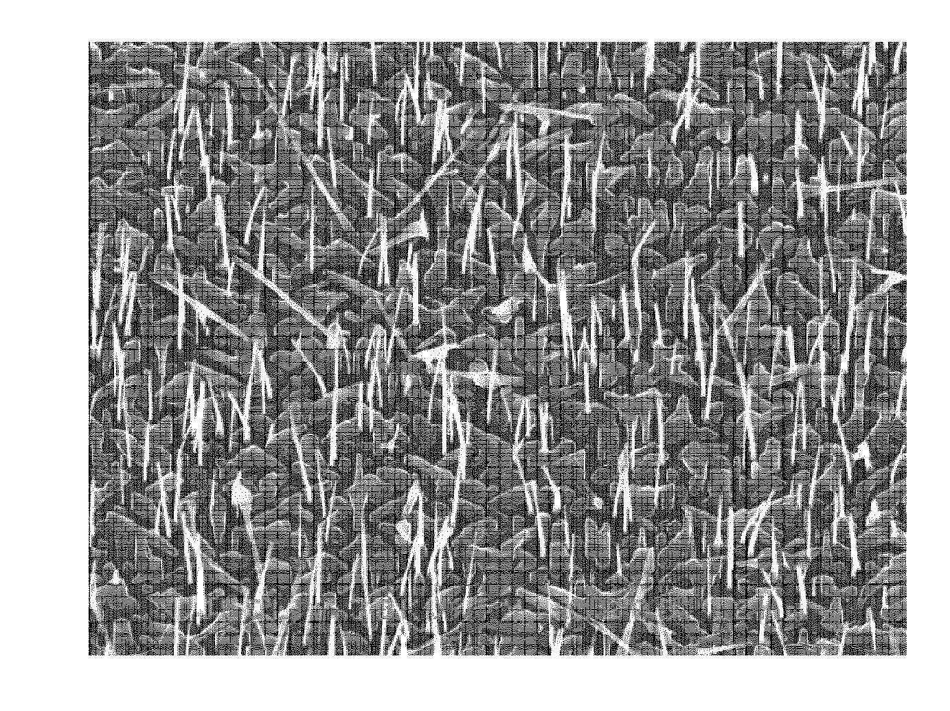
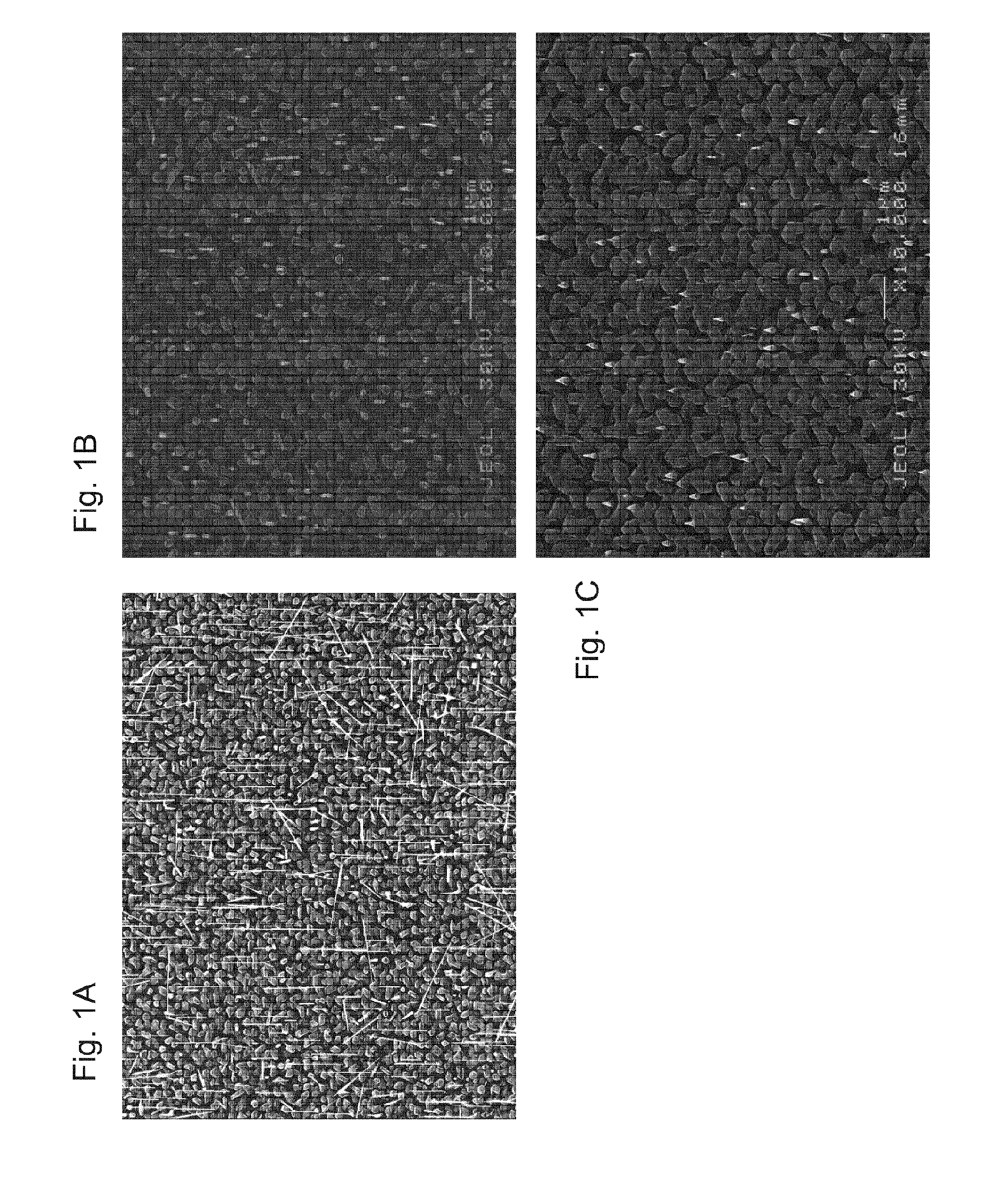
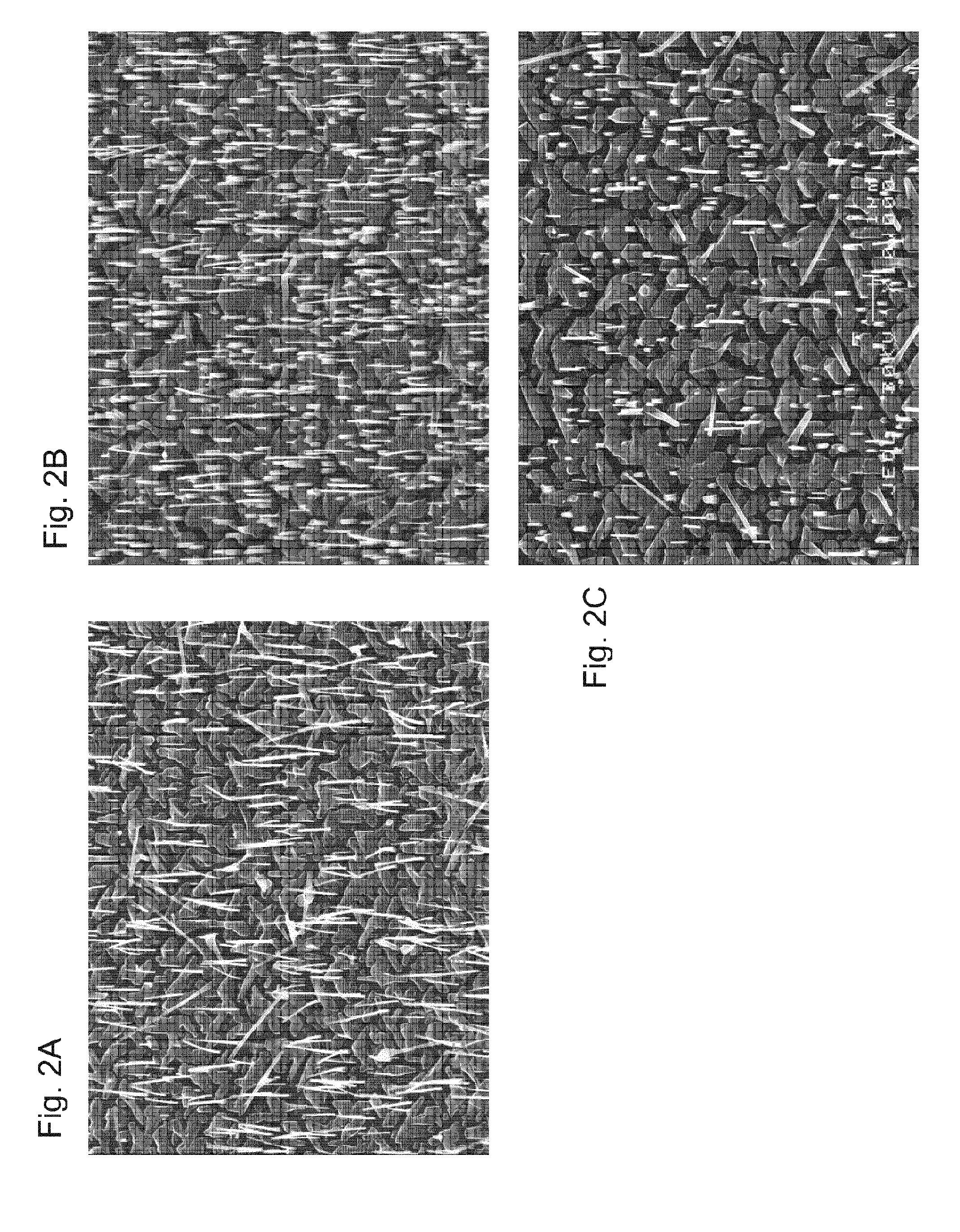
[0050]FIGS. 1A, 1B and 1C show three nanostructure growths which illustrate that the maximum group V / III ratio which can be used in the MBE configuration for these Ga-assisted GaAsP growth is lower than what can be used for the known Ga-assisted GaAs growth.

[0051]The experimental parameters used for the growths shown in FIGS. 1A, 1B and 1C are shown in the following tables. The flux parameters are expressed as beam equivalent pressures in Torr (1 Torr being approximately 133.3 Pa). The growth temperatures were measured with a pyrometer.

TimeTemperatureFIG. 1AGa fluxAs fluxP flux(mins)(° C.)Growth8.72 × 10−81.06 × 10⁻⁵—20630

TimeTemperatureFIG. 1BGa fluxAs fluxP flux(mins)(° C.)Growth8.72 × 10−85.3 × 10−65.3 × 10−620630

Tem-pera-TimetureFIG....


PUM

PropertyMeasurementUnit
band gapaaaaaaaaaa
temperatureaaaaaaaaaa

Abstract

The application discloses a technique for fabricating gallium-arsenide-phosphorous (GaAsP) nanostructures using gallium-assisted (Ga-assisted) Vapour-Liquid-Solid (VLS) growth, i.e. without requiring gold catalyst particles. The resulting Ga-assisted GaAsP nanostructures are free of gold particles, which renders them useful for optoelectronic applications, e.g. as a junction in a solar cell. The Ga-assisted GaAsP nanostructures can be fabricated with a band gap in the range 1.6 to 1.8 eV (e.g. at and around 1.7 eV).

Description

FIELD OF THE INVENTION[0001]The invention relates to semiconductor nanostructures, such as nanowires or nano “flakes”, and is applicable, for example, in photovoltaic devices or the like.BACKGROUND TO THE INVENTION[0002]Conventionally, a nanostructure is a material structure having at least one region or characteristic dimension whose size is in the nanometre range (i.e. ˜10−9 m). For example, the structure may be in the form of a plate whose thickness is in the nanometre range. Alternatively, the structure may be substantially one dimensional, wherein its transverse dimension is in the nanometre range. Quasi-one-dimensional nanostructure may be referred to as nanowires.[0003]Growth of semiconductor nanowires was first discussed in 1964 by Wagner and Ellis. The nanowires they grew were catalyzed by means of a liquid gold catalyst particle and a nanowire growth mechanism named Vapour-Liquid-Solid (VLS) growth mechanism. This name derives from the fact that material(s) used for growin...

Claims


Application Information

Patent Timeline
Patent Type & Authority Applications(United States)
IPC IPC(8): H01L31/0352H01L21/02H01L31/0304H01L29/20H01L29/06
CPCH01L31/035227H01L29/20H01L29/0669H01L31/03046H01L21/02488H01L21/02546H01L21/02653H01L21/02381H01L21/02543H01L21/02461H01L21/02463H01L21/02513H01L21/02573H01L21/02603H01L21/02645H01L29/0676H01L31/0687H01L31/1852Y02E10/544
Inventor AAGESEN, MARTINJORGENSEN, HENRIK INGERSLEVHOLM, JEPPE VILSTRUPSCHALDEMOSE, MORTEN
Owner GASP SOLAR APS
Why Eureka
Try Eureka