Module, electronic apparatus, moving object, and method of manufacturing module

a technology of electronic equipment and manufacturing methods, applied in the field of modules, electronic equipment, moving objects, and manufacturing modules, can solve the problems of increasing the cost of the semiconductor device (the module), and achieve the effects of increasing cost, stable characteristics, and low cos

Active Publication Date: 2014-09-25
COLUMBIA PEAK VENTURES LLC
View PDF6 Cites 9 Cited by
  • Summary
  • Abstract
  • Description
  • Claims
  • Application Information

AI Technical Summary

Benefits of technology

[0010]According to this application example, the projection section is disposed so that the distance between the projection section and the second base member on the tip side of the projection section is longer than the distance between the projection section and the second base member on the principal surface side. In other words, the shorter the distance from the principal surface is, the shorter the distance between the projection section and the second base member is, and the higher the surface tension with the bonding material having flown becomes. Thus, it becomes possible to enhance the stopping effect of the bonding material in the part near to the principal surface, and thus, the flow of the bonding material can more reliably be stopped.Application Example 3
[0012]According to this application example, since the side surface of the second base member is formed as a slope, the outflow resistance of the bonding material having flown is increased, or the plane area is increased due to the slope to elongate the outflow length. Therefore, it becomes possible to reduce the amount of the bonding material, which reaches the projection section, and the flow of the bonding material can more surely be stopped by the projection section.Application Example 4
[0014]According to this application example, since the second functional element is connected so as to project from the top surface of the second base member toward the electrode, the distance between the second functional element and the projection section in the plan view is decreased, and the distance between the second functional element and the electrode in the plan view is also decreased. Thus, it becomes easy for the wiring lines to stride over the projection section, thus the wiring lines can be prevented from having contact with the projection section, and at the same time, the wiring lines between the second functional element and the electrodes can be shortened, and thus, it becomes easy to form a wiring shape.Application Example 5
[0022]According to this present application example, it becomes possible to provide an electronic apparatus low in cost and stable in characteristics using the module suppressing increase in cost, and capable of inhibiting the contamination of the electrode by the bonding material.Application Example 9
[0024]According to this present application example, it becomes possible to provide a moving object low in cost and stable in characteristics using the module suppressing increase in cost, and capable of inhibiting the contamination of the electrode by the bonding material.

Problems solved by technology

In other words, it results that the man-hour for forming the dam is required additionally, which contributes to the increase in cost of the semiconductor device (the module).

Method used


Image

  • Module, electronic apparatus, moving object, and method of manufacturing module
  • Module, electronic apparatus, moving object, and method of manufacturing module
  • Module, electronic apparatus, moving object, and method of manufacturing module

Examples


first embodiment

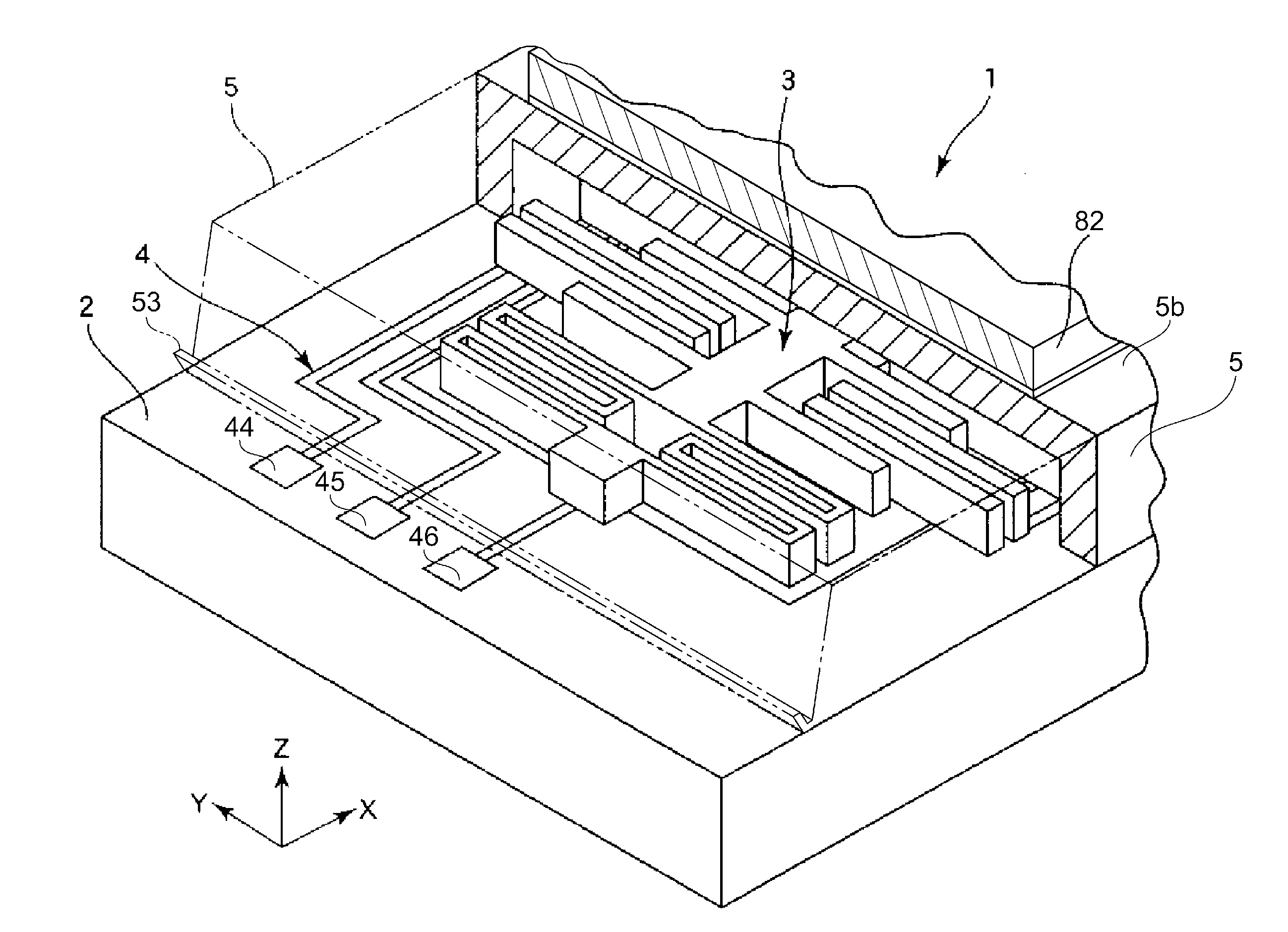
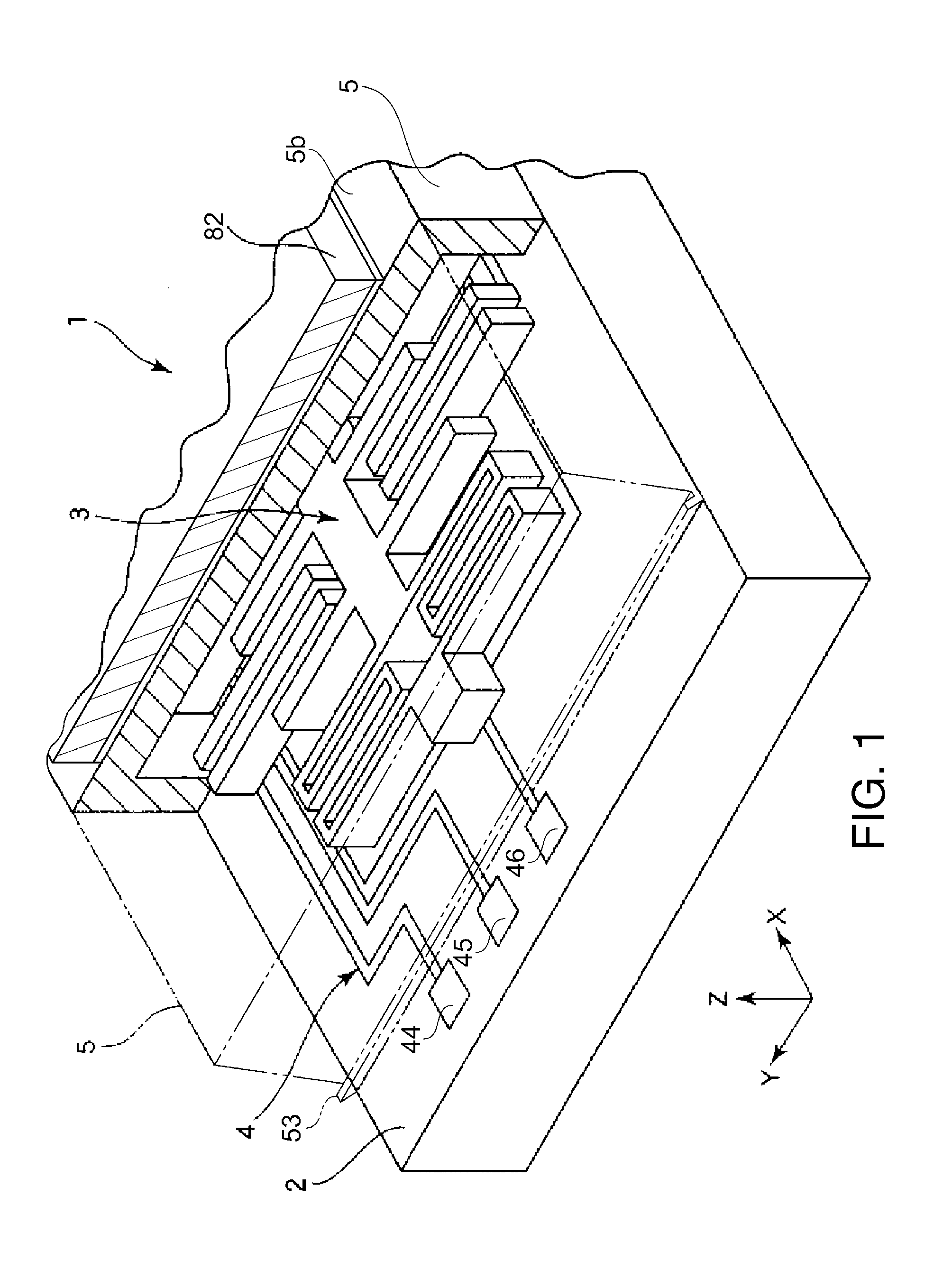
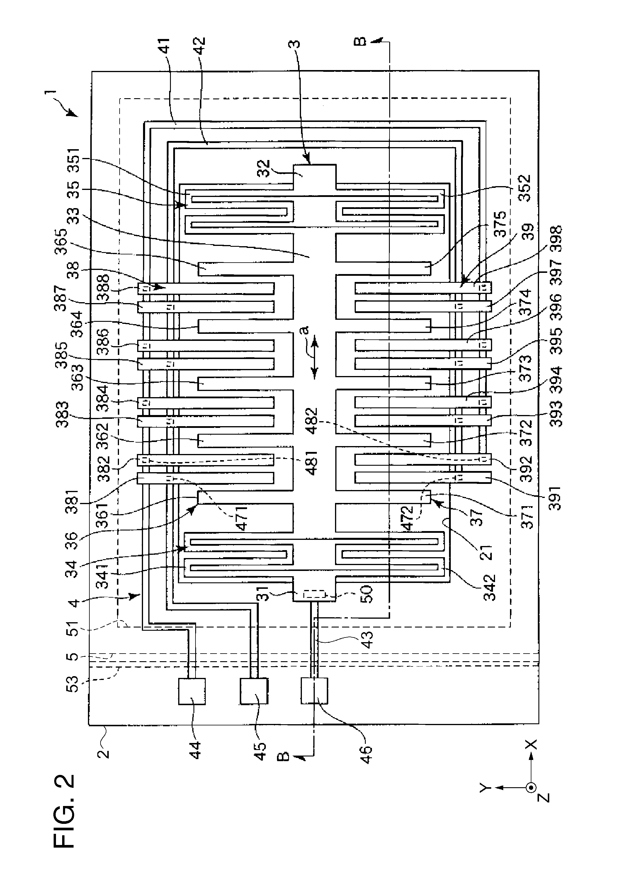
[0036]A module according to the first embodiment of the invention will be explained using FIGS. 1 through 3. FIG. 1 is a perspective view schematically showing the module according to the first embodiment of the invention. FIG. 2 is a plan view schematically showing the module shown in FIG. 1, and is a diagram with a lid member omitted (viewed through the lid member). FIG. 3 is a cross-sectional view along the B-B line showing the module shown in FIG. 2. It should be noted that in FIGS. 1 and 3, the X axis, the Y axis, and the Z axis are shown as three axes perpendicular to each other. Hereinafter, a direction (a horizontal direction) parallel to the X axis is referred to as an “X-axis direction,” a direction parallel to the Y axis is referred to as a “Y-axis direction,” and a direction (a vertical direction) parallel to the Z axis is referred to as a “Z-axis direction.” Further, the near side (in the Z-axis direction) of the sheet of FIG. 2 is referred to as an “upper side,” the fa...

second embodiment

[0114]A module according to a second embodiment of the invention will be explained using FIGS. 5A and 5B. FIGS. 5A and 5B are diagrams schematically showing the module according to the second embodiment of the invention, wherein FIG. 5A is a plan view, and FIG. 5B is a front cross-sectional view. It should be noted that in the explanation of the second embodiment, the same constituents as in the first embodiment described above are denoted with the same reference symbols, and the explanation thereof will be omitted. It should be noted that FIG. 5A shows a state of eliminating a mold member constituting the module.

[0115]The module 80 shown in FIG. 5 is provided with a base substrate 81, the insulating substrate 2 as the first base member connected to the base substrate 81, the device element 3 as the first functional element bonded to and supported by the insulating substrate 2, and the lid member 5 as the second base member disposed so as to cover the device element 3. Further, the ...


PUM

PropertyMeasurementUnit
thicknessaaaaaaaaaa
thicknessaaaaaaaaaa
areaaaaaaaaaaa

Abstract

A module includes an insulating substrate having an upper surface as a principal surface, a lid member having an internal space with the insulating substrate, and bonded to the upper surface in a first surface, a device element housed in the internal space, a semiconductor element connected to a top surface, which forms the both sides of the lid member together with the first surface, using a resin adhesive, electrodes electrically connected to the device element, and disposed on an upper surface of the insulating substrate in an area other than the connection area with the lid member, and a projection section formed of the same member as the lid member on the upper surface in an area between the electrodes and the lid member in a plan view.

Description

BACKGROUND[0001]1. Technical Field[0002]The invention relates to a module, a method of manufacturing the module, an electronic apparatus using the module, and a moving object.[0003]2. Related Art[0004]In the past, as an example of a module, there has been proposed a semiconductor device having a semiconductor chip as a functional element mounted on a base substrate. In this semiconductor device, as a method of connecting the base substrate and the semiconductor chip to each other, there are used a flip-chip connection using, for example, a solder bump or a gold bump, a die attachment using a resin adhesive, and so on. In the flip-chip connection, the gap between the semiconductor chip and the base substrate is filled with resin called underfill resin. Further, in the die attachment, there is disposed a resin adhesive between the semiconductor chip and the base substrate. The underfill resin and the resin adhesive are high in fluidity, and in some cases, the resin component flows out...

Claims


Application Information

Patent Timeline
Patent Type & Authority Applications(United States)
IPC IPC(8): H05K7/06H05K3/04
CPCH05K3/04H05K7/06H01L2224/48091H01L2224/48465H01L23/147H01L23/15G01P1/023G01P15/125G01C19/5769Y10T29/49156H01L2924/00014H01L2924/00
Inventor KOBAYASHI, TOMONAGA
Owner COLUMBIA PEAK VENTURES LLC
Why Eureka
Try Eureka