

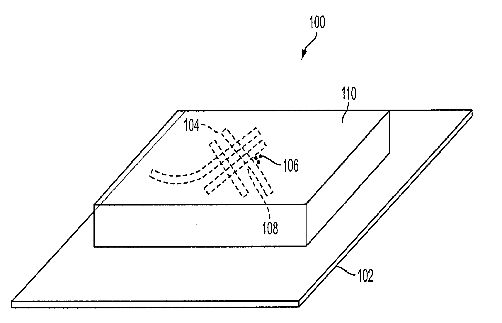
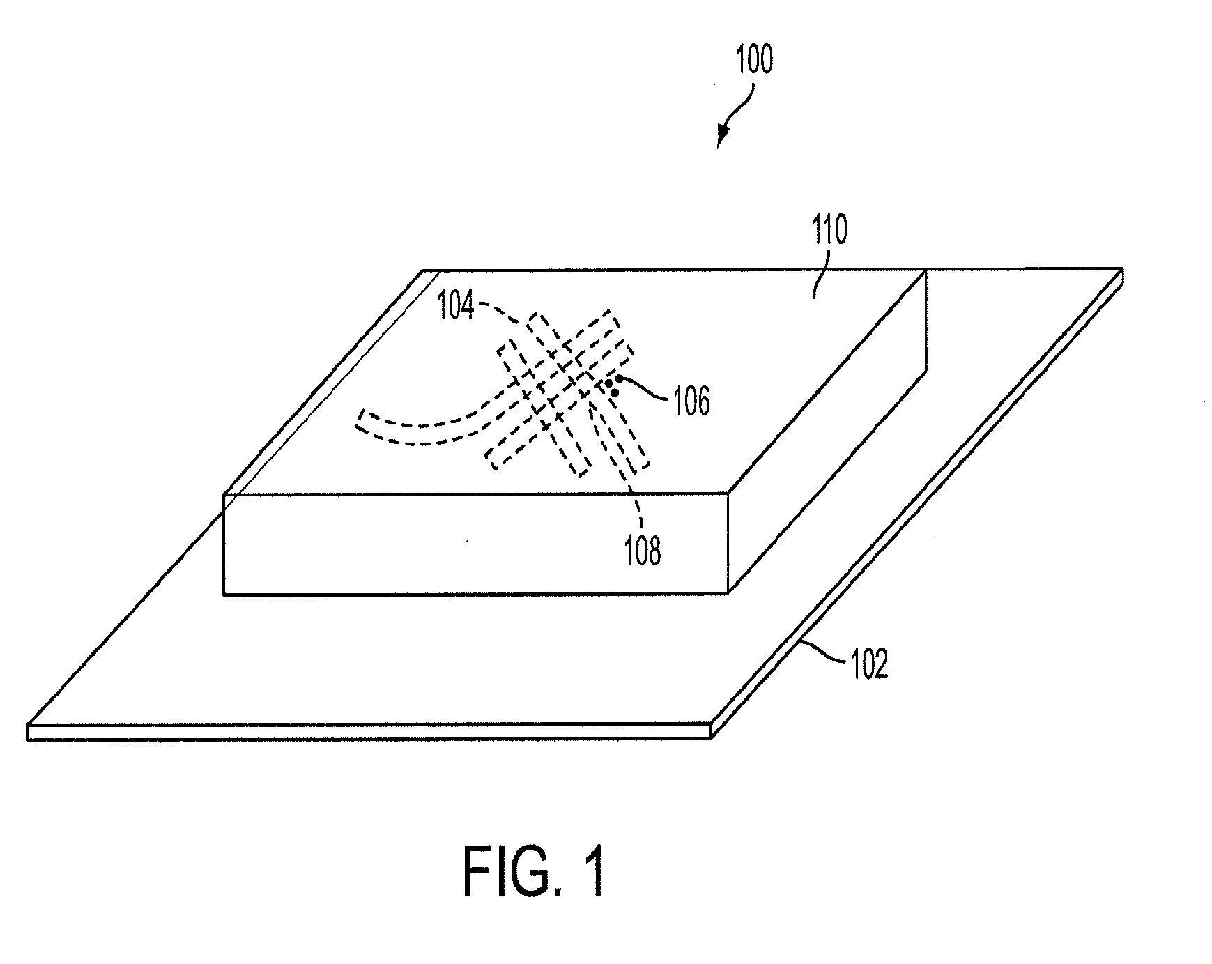
Solution processed nanoparticle-nanowire composite film as a transparent conductor for opto-electronic devices
a composite film and nanoparticle technology, applied in the direction of sustainable manufacturing/processing, instruments, final product manufacturing, etc., can solve the problems of optical transparency and electrical conductivity compromise, not providing transparent electrodes and methods of production
- Summary
- Abstract
- Description
- Claims
- Application Information
AI Technical Summary
Benefits of technology
Problems solved by technology
Method used
Image

Examples
examples
[0033]The following examples help explain some concepts of the current invention. However, the general concepts of the current invention are not limited to the particular examples.
[0034]Sputter-deposited indium tin oxide (ITO) or Al-doped zinc oxide are commonly used as transparent conductors for thin film optoelectronic devices such as displays and thin film solar cells because those films provide both low resistance and high transmittance (Hoel C. A; Mason T. O., Gaillard J.-F.; Poeppelmeier K. R. Chem. Mater. 2010, 22, 3569). Due to high manufacturing cost inherent from the use of vacuum techniques in the preparation of conventional transparent conductors, non-vacuum processing methods have been studied to reduce the cost (Gordon R. G. MRS bulletin 2000, 25, 52). Although solution processed silver nano-wire (AgNW) has pursued as a potential alternative, these films have shown poor adhesion to adjacent layers (De, S.; Higgins, T. M.; Lyons, P. E.; Doherty, E. M.; Nirmalraj, P. N.;...
PUM
| Property | Measurement | Unit |
|---|---|---|
| temperature | aaaaa | aaaaa |
| temperature | aaaaa | aaaaa |
| temperature | aaaaa | aaaaa |
Abstract
Description
Claims
Application Information