This helps you quickly interpret patents by identifying the three key elements:
Problems solved by technology
Method used
Benefits of technology
Benefits of technology
The present invention provides a thin ceramic electronic component that is resistant to moisture.
Problems solved by technology
As a result, the conductive paste cannot be sufficiently applied to the ridge portions of the capacitor body and, in some cases, the terminal electrodes are not appropriately formed in the ridge portions of the capacitor body.
This poses a problem in that moisture and the like enter the capacitor body through a portion in which the terminal electrodes are not formed, which degrades the moisture resistance.
Image
Click on the blue label to locate the original text in one second.
Reading with bidirectional positioning of images and text.
Examples
first preferred embodiment
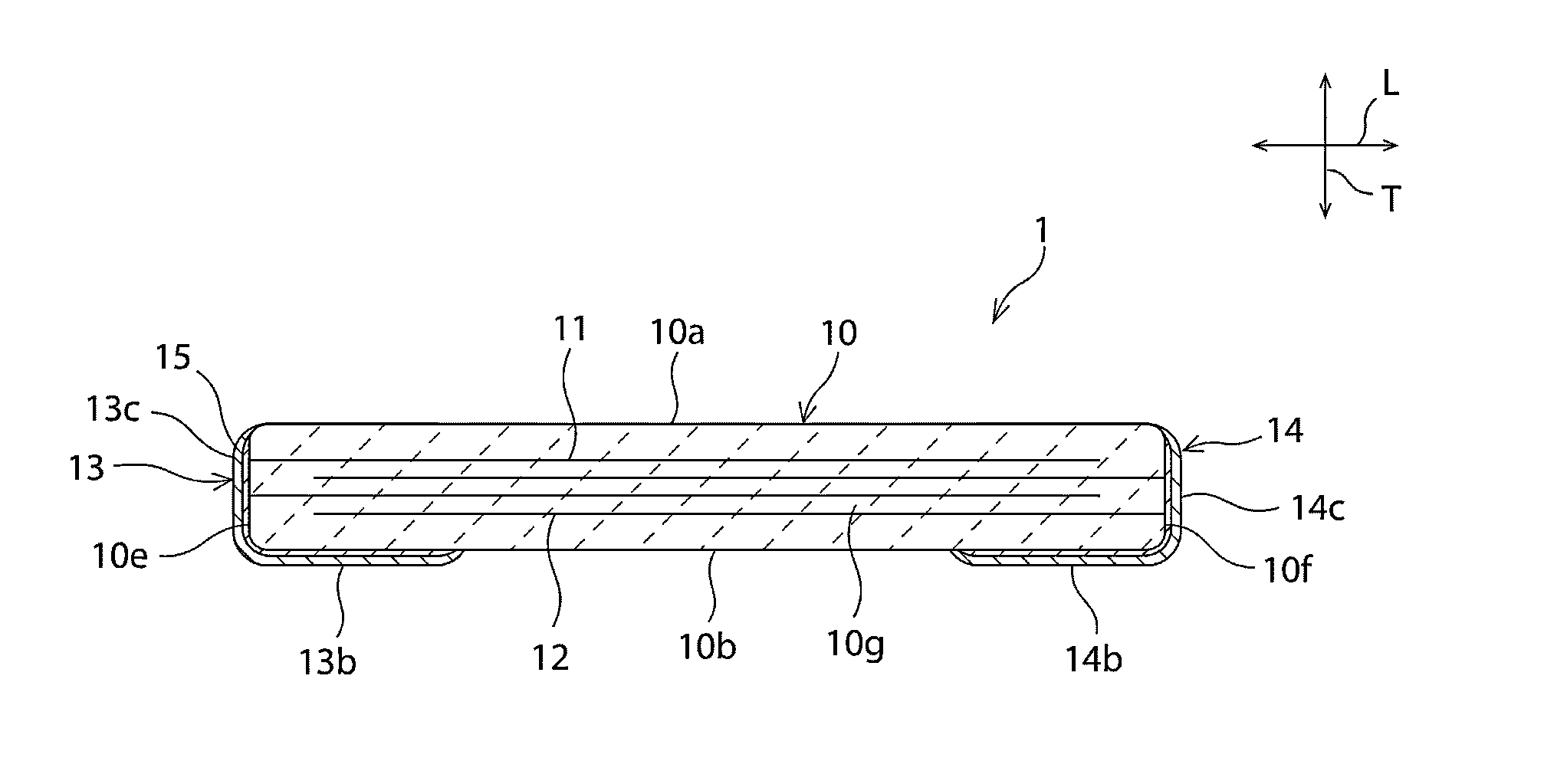
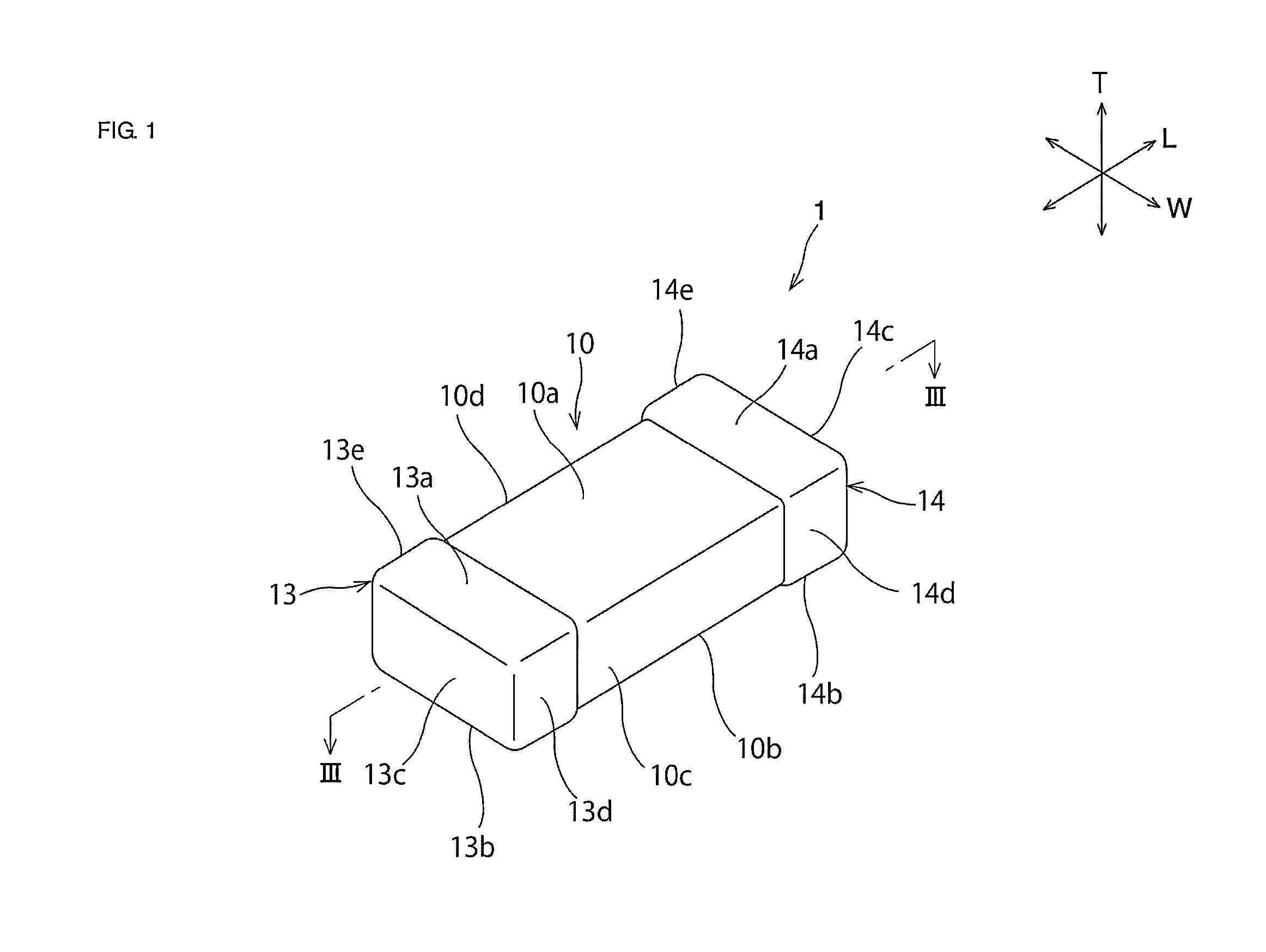
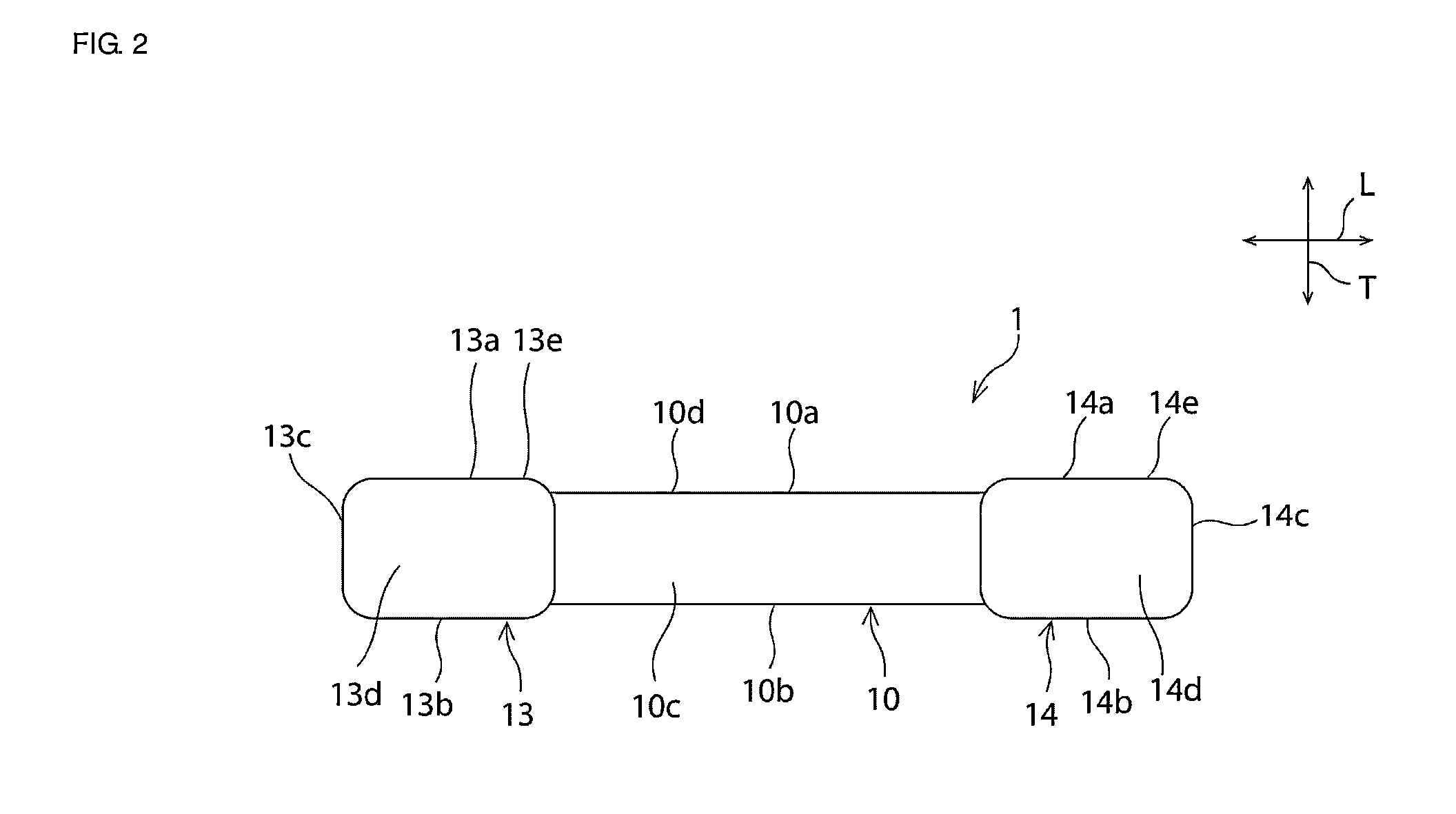
[0037]FIG. 1 is a schematic perspective view of a ceramic electronic component according to the first preferred embodiment of the present invention. FIG. 2 is a schematic side view of the ceramic electronic component according to this preferred embodiment. FIG. 3 is a schematic sectional view taken along line III-III of FIG. 1. FIG. 4 is a schematic sectional view in which a portion enclosed with line IV of FIG. 3 is enlarged. FIG. 5 is a schematic sectional view showing a glass coating layer and a first outer electrode of a ceramic electronic component produced in this preferred embodiment. FIG. 7 is a schematic sectional view taken along line VII-VII of FIG. 3.
[0038]A structure of a ceramic electronic component 1 will be described with reference to FIGS. 1 to 7.
[0039]As illustrated in FIGS. 1 to 3 and 7, the ceramic electronic component 1 includes a ceramic body 10. The ceramic body 10 preferably is composed of an appropriate ceramic material that provides the functions of the cer...
second preferred embodiment
[0114]FIG. 11 is a schematic perspective view of a ceramic electronic component according to a second preferred embodiment of the present invention.
[0115]In the first preferred embodiment, an example in which the first and second outer electrodes 13 and 14 and the glass coating layers 15 are preferably located on the first and second side surfaces 10c and 10d has been described. However, as illustrated in FIG. 11, the first and second outer electrodes 13 and 14 and the glass coating layers 15 are not necessarily located on the first and second side surfaces 10c and 10d.
[0116]The ceramic electronic component according to the second preferred embodiment can be produced by, for example, the following method. A mother multilayer body 22 (refer to FIG. 12) is obtained in the same manner as the method for producing the ceramic electronic component 1 according to the first preferred embodiment. In this preferred embodiment, as illustrated in FIG. 12, a conductive pattern 23 having a shape...
third preferred embodiment
[0119]FIG. 13 is a schematic sectional view of a ceramic electronic component according to a third preferred embodiment of the present invention.
[0120]In the first preferred embodiment, an example in which the first and second outer electrodes 13 and 14 and the glass coating layers 15 are preferably located on the first and second principal surfaces 10a and 10b has been described. However, the present invention is not limited to the structure. The first and second outer electrodes 13 and 14 and the glass coating layers 15 may each be located on any portion on the surface of the ceramic body 10.
[0121]For example, as illustrated in FIG. 13, the first and second outer electrodes 13 and 14 and the glass coating layers 15 may be located on only the second principal surface 10b among the first and second principal surfaces 10a and 10b.
PUM
Abstract
A ceramicelectronic component includes a ceramic body, inner electrodes, a glass coating layer, and outer electrodes. The glass coating layer extends from an exposed portion of one of the inner electrodes at a first end surface to a first principal surface. The outer electrodes are each constituted by a plating film disposed directly above the glass coating layer. The glass coating layer includes a glass medium and metalpowder particles that define conductive paths. The metalpowder particles have an elongated or substantially elongated shape and are dispersed in the glass medium. The dimension of a portion of the glass coating layer located on the first principal surface in the length direction, is larger than that of a portion of the glass coating layer located on the first end surface in the thickness direction.
Description
BACKGROUND OF THE INVENTION[0001]1. Field of the Invention[0002]The present invention relates to a ceramicelectronic component.[0003]2. Description of the Related Art[0004]Hitherto, ceramic electronic components such as ceramic capacitors have been used for electronic devices such as cellular phones and portable music players. For example, as described in Japanese Unexamined Patent Application Publication No. 2011-100834, a ceramic electronic component generally includes a ceramic body having a surface at which an end portion of each of inner electrodes is exposed and outer electrodes disposed so as to cover a portion of the ceramic body in which the inner electrode is exposed.[0005]However, in ceramic electronic components in which side surface electrodes of terminal electrodes are formed so as to extend to near a central portion of a capacitor body and have a large length as illustrated in FIG. 1 of Japanese Unexamined Patent Application Publication No. 2011-100834, for example, ...
Claims
Application Information
Patent Timeline
Application Date:The date an application was filed.
Publication Date:The date a patent or application was officially published.
First Publication Date:The earliest publication date of a patent with the same application number.
Issue Date:Publication date of the patent grant document.
PCT Entry Date:The Entry date of PCT National Phase.
Estimated Expiry Date:The statutory expiry date of a patent right according to the Patent Law, and it is the longest term of protection that the patent right can achieve without the termination of the patent right due to other reasons(Term extension factor has been taken into account ).
Invalid Date:Actual expiry date is based on effective date or publication date of legal transaction data of invalid patent.

