Cpp-type magnetoresistance effect element and magnetic disk device using side shield layers
a magnetoresistance effect and magnetic disk technology, applied in the direction of recording information storage, maintaining head carrier alignment, instruments, etc., can solve the problems of limited operating current from a reliability perspective, limited area of the element, and reduced sensitivity, so as to improve the linear recording density and improve sensitivity
- Summary
- Abstract
- Description
- Claims
- Application Information
AI Technical Summary
Benefits of technology
Problems solved by technology
Method used
Image
Examples
experimental example 1
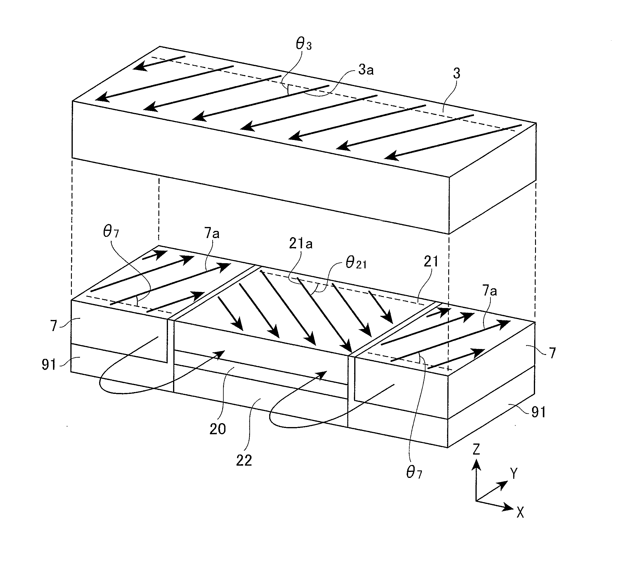
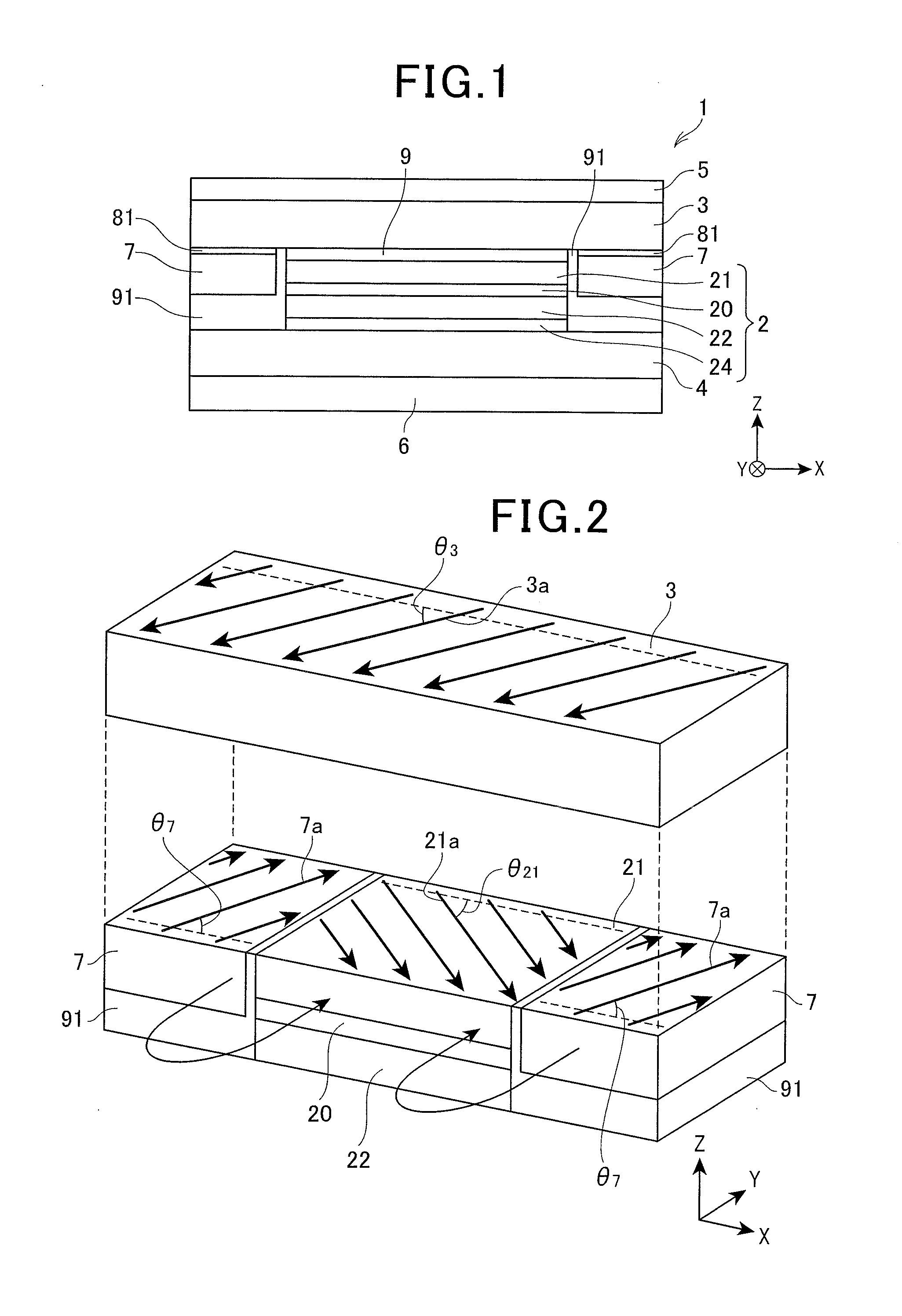
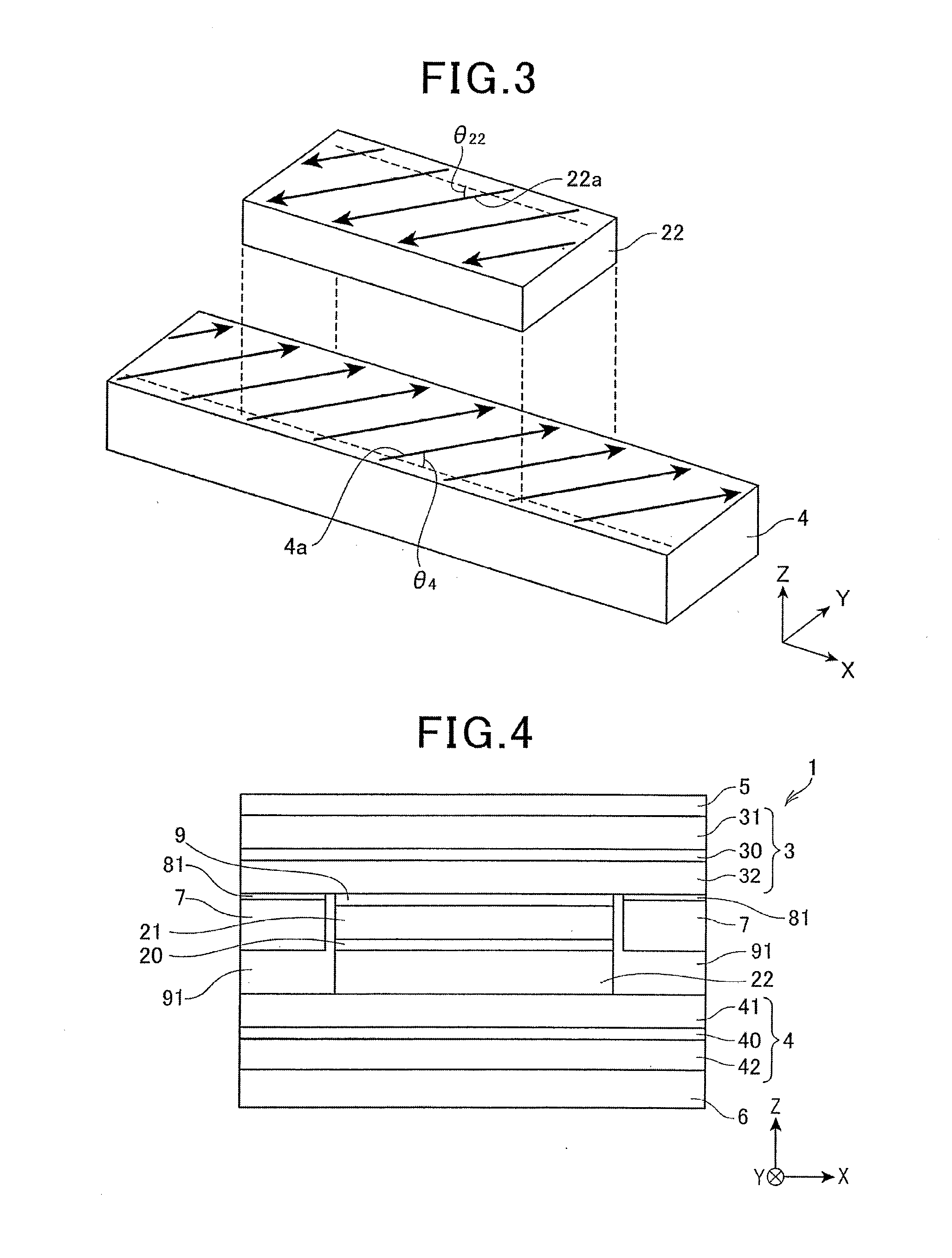
[0180]For the angle θ21 of the magnetization 21a of the first ferromagnetic layer 21 when the angle θ2 of the magnetization 7a of the side shield layer 7 in the MR element 1 having the configuration shown in FIG. 4 was fluctuated within a predetermined range, a simulation analysis experiment (calculation of an angle of magnetization by LLG simulation) was conducted.
[0181]In the MR element 1 used in this simulation analysis experiment, the first upper shield layer 31, the second upper shield layer 32 and the side shield layer 7 were all regarded as magnetization pinned layers where the angles θ3 and θ7 of their magnetizations 31a, 32a and 7a were pinned at a predetermined angle(s), respectively. Further, the first lower shield layer 41 and the second lower shield layer 42 were regarded as magnetization pinned layers where the angle θ4 of their magnetizations 41a and 42a were pinned to 45 degrees, respectively, and the magnetizations 41a and 42a were in an antiparallel state to each o...
experimental example 2
[0183]In the MR element 1 of Experimental example 1, without pinning the angle θ22 of the magnetization 22a of the second ferromagnetic layer 22, the simulation analysis experiment (calculation of an angle of magnetization by the LLG simulation) was conducted as similar to Example 1.
[0184]In the MR element 1 used in this simulation analysis experiment, the first upper shield layer 31, the second upper shield layer 32 and the side shield layer 7 were regarded as magnetization pinned layers where the angles θ3 and θ7 of the magnetizations 3a and 7a were pinned to 68.3 degrees. Further, the first lower shield layer 41 and the second lower shield layer 42 were regarded as magnetization pinned layers where the angle θ4 of their magnetizations 41a and 42a was pinned to a predetermined angle.
Furthermore, the intensity of exchange-coupling J (erg / cm2) between the second lower shield layer 42 and the second ferromagnetic layer 22 in the MR element 1 was set at −0.2 erg / cm2.
[0185]A graph show...
experimental example 3
[0186]In the MR element 1 shown in FIG. 4 and FIG. 6A, for the angles θ21 and θ22 of the magnetizations 21a and 22a of the first ferromagnetic layer 21 and the second ferromagnetic layer 22 when the thickness T71b of the second side shield layer 71b became fluctuated without pinning the angles θ21 and θ22 of the magnetizations 21a and 22a of the first ferromagnetic layer 21 and the second ferromagnetic layer 22, a simulation analysis experiment (calculation of an angle of magnetization by LLG simulation) was conducted.
[0187]In the MR element 1 used in this simulation analysis experiment, the first upper shield layer 31, the second upper shield layer 32 and the side shield layer 7 were regarded as magnetization pinned layers where the angles θ3 and θ7 of the magnetizations 31a, 32a and 7a were pinned to 68.3 degrees. Further, the first lower shield layer 41 and the second lower shield layer 42 were regarded as magnetization pinned layers where the angle θ4 of the magnetizations 41a a...
PUM
 Abstract
Description
Claims
Application Information


