SINGLE-CRYSTAL 4H-SiC SUBSTRATE AND METHOD FOR MANUFACTURING THE SAME
a single-crystal, 4hsic technology, applied in the direction of crystal growth process, polycrystalline material growth, transportation and packaging, etc., can solve the problem of not having a known method for reducing crystal defects, and achieve the effect of reducing the density of crystal defects
- Summary
- Abstract
- Description
- Claims
- Application Information
AI Technical Summary
Benefits of technology
Problems solved by technology
Method used
Image
Examples
first embodiment
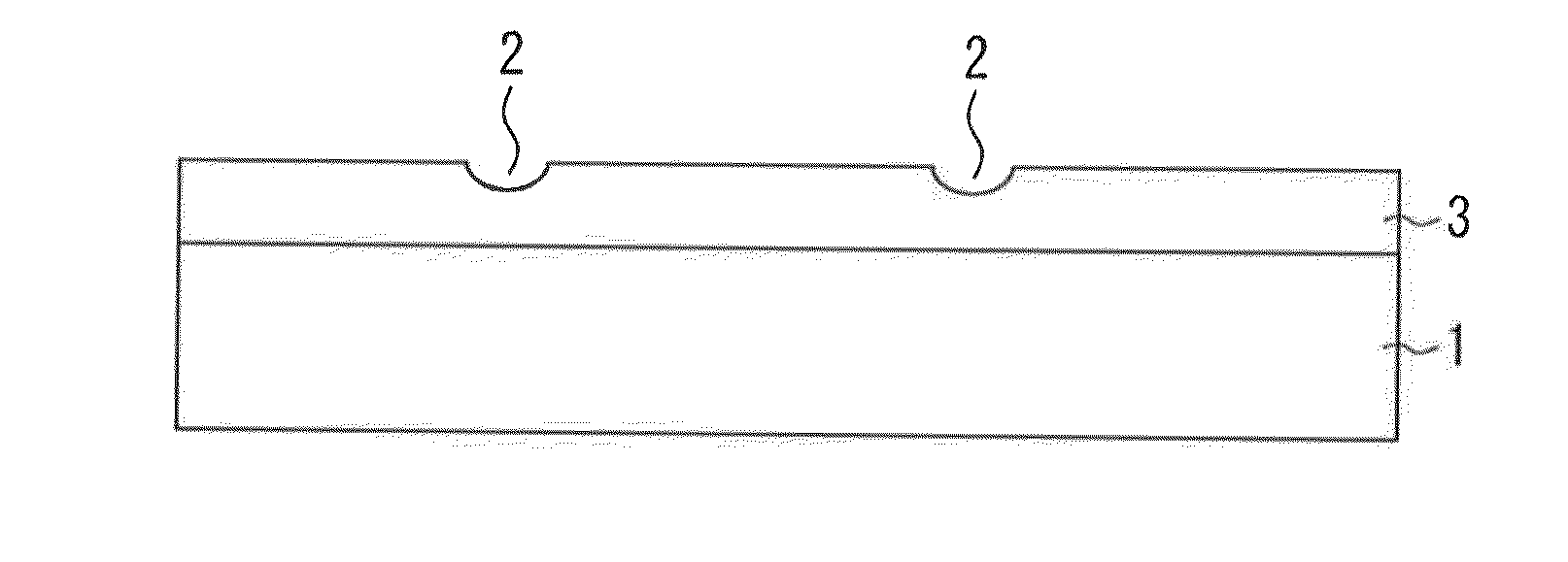
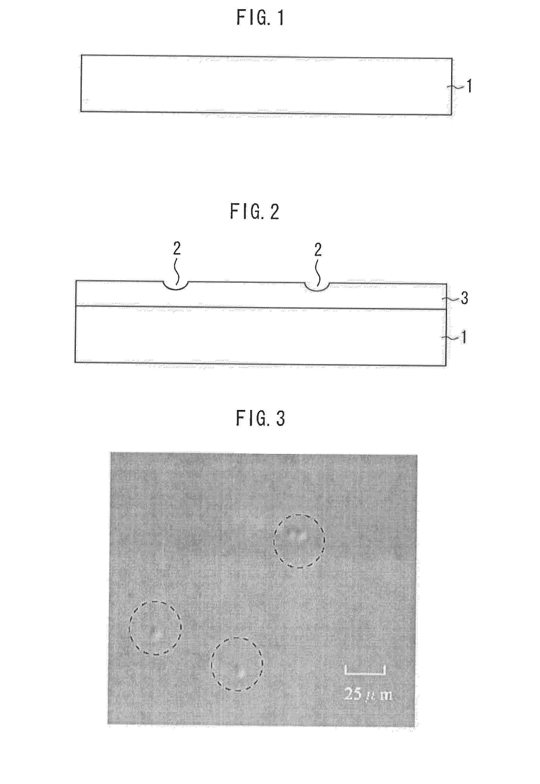
[0020]A method of manufacturing a single-crystal 4H-SiC substrate in accordance with a first embodiment of the present invention will be described. FIGS. 1 and 2 are cross-sectional views showing the method of manufacturing a single-crystal 4H-SiC substrate in accordance with the first embodiment. The method begins by preparing a 4H-SiC bulk single-crystal substrate 1 misoriented by 4 degrees from the (0001) plane (or C-plane) toward a direction, as shown in FIG. 1. (The completed single-crystal 4H-SiC substrate of the present embodiment will have a principal surface in the (0001) plane.) It should be noted that the misorientation angle need not necessarily be 4 degrees, but may be in the range of 2-10 degrees.
[0021]Specifically, the 4H-SiC bulk single-crystal substrate 1 is planarized by mechanical polishing and chemical mechanical polishing using an acidic or alkaline solution. Further, the substrate 1 is ultrasonically cleaned using acetone to remove organic matter. The 4H-SiC b...
second embodiment
[0028]A method of manufacturing a single-crystal 4H-SiC substrate in accordance with a second embodiment of the present invention will be described. FIG. 7 is a cross-sectional view showing the method of manufacturing a single-crystal 4H-SiC substrate in accordance with the second embodiment.
[0029]First, as in the first embodiment, a single-crystal 4H-SiC layer 3 having a thickness of 300 nm is epitaxially grown so that that its growth surface has recesses 2. It should be noted that the thickness of the single-crystal 4H-SiC layer 3 need not necessarily be 300 nm, but may be in the range of from 50 nm to 10 μm. Then, as shown in FIG. 7, a single-crystal 4H-SiC layer 4 having a thickness of 10 μm is epitaxially grown on the single-crystal 4H-SiC layer 3 so as to bury the recesses 2.
[0030]Specifically, the single-crystal 4H-SiC layer 4 is formed by supplying SiH4 gas at a flow rate of 900 sccm and C3H8 gas at a flow rate of 360 sccm and further supplying nitrogen gas serving as an N-t...
PUM
| Property | Measurement | Unit |
|---|---|---|
| misorientation angle | aaaaa | aaaaa |
| misorientation angle | aaaaa | aaaaa |
| diameter | aaaaa | aaaaa |
Abstract
Description
Claims
Application Information


