

Method for high resolution sum-frequency generation and infrared microscopy
a sum-frequency generation and infrared microscopy technology, applied in the field of microscopy, can solve the problems of inability to achieve resolutions in the micrometer range in far-field ir microscopy, and inability to achieve spatial resolution better, and the diffraction limitation of far-field imaging approaches
- Summary
- Abstract
- Description
- Claims
- Application Information
AI Technical Summary
Benefits of technology
Problems solved by technology
Method used
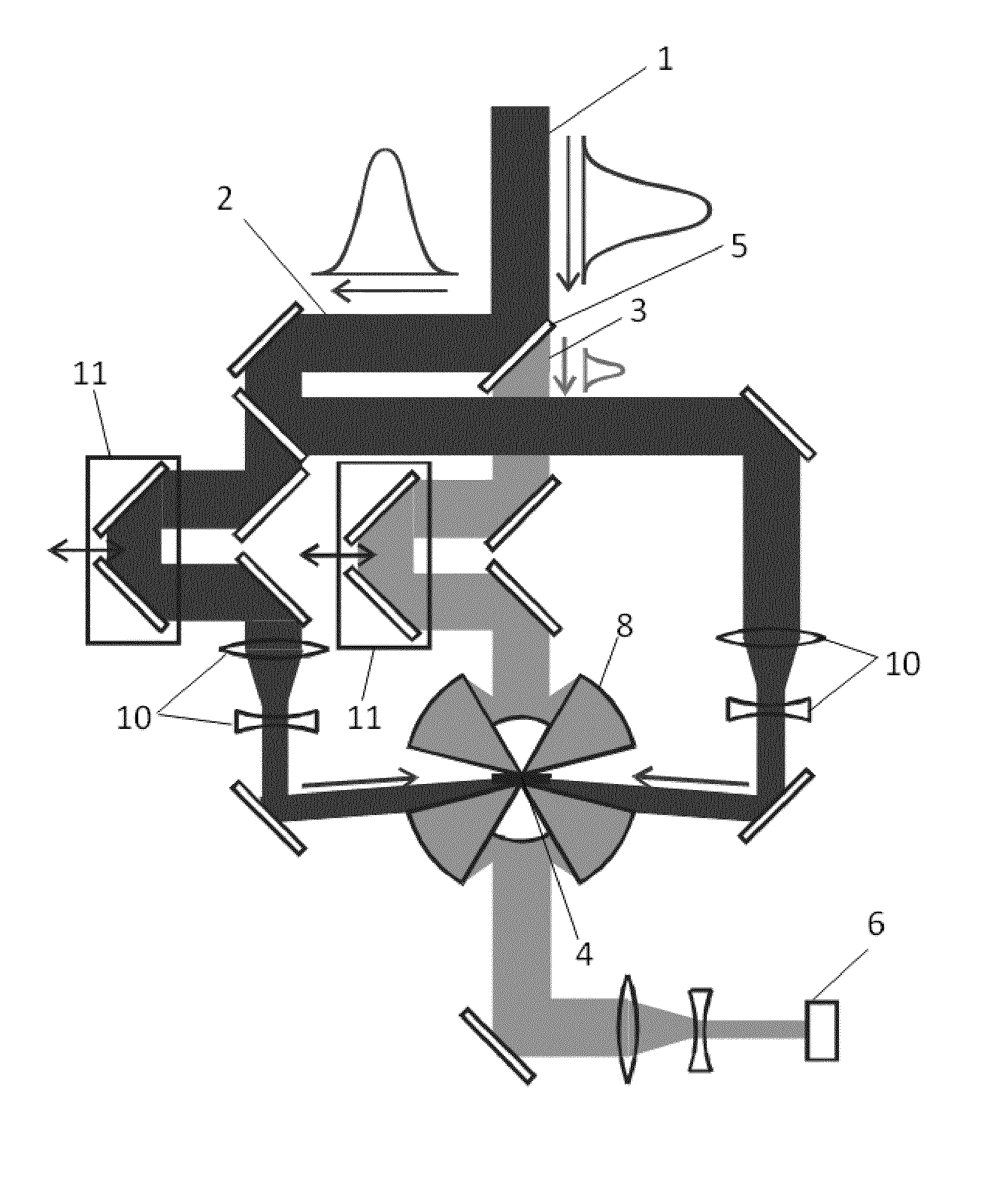
Image

Examples
example
[0107]The following example illustrates how to use the method to record the IRN (or ASM IR) signal.
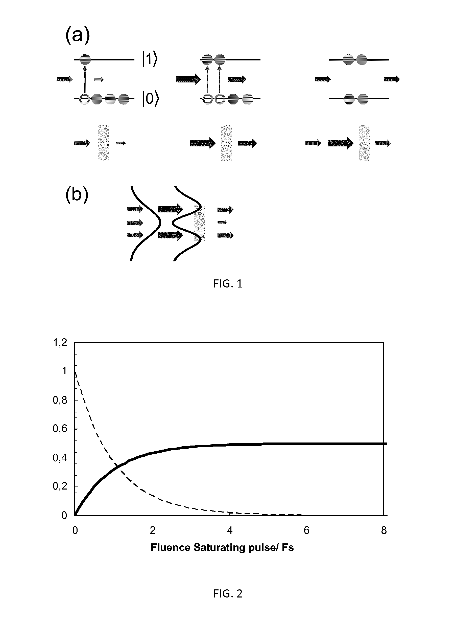
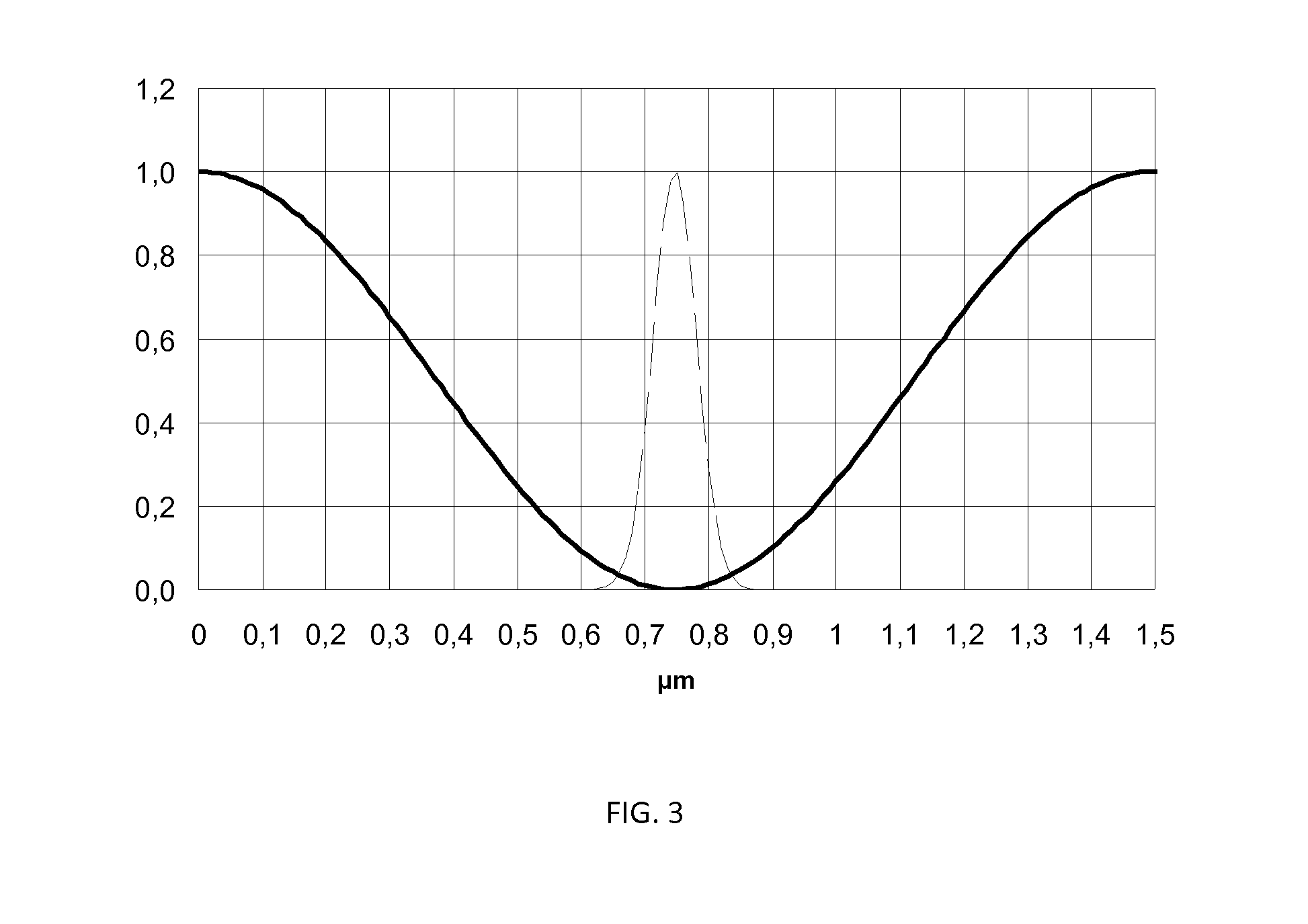
[0108]This example illustrates a computed simulation of the mapping of a vibrational mode absorption with a resolution below the diffraction limit, and defines an example of IRN point-spread function (PSF). To define the PSF in this example, one uses two different intensity profiles for the pump and one records / integrates the intensity / energy of the probe in both cases.
[0109]The difference between probe intensities is defined in this example as the IRN signal and has a PSF that is punctual and has a below-the-diffraction-limit full-width at half maximum (i.e., the fwhm is a measure of the microscope resolution). The discussion concerns a measure in transmission geometry but also applies to a measure in reflection geometry.
[0110]The following IRN PSF simulation uses a simplified model of Einstein for the absorption.
[0111]A sample corresponding to a self-assembled film of octadecylsilane...
PUM
| Property | Measurement | Unit |
|---|---|---|
| wavelength | aaaaa | aaaaa |
| wavelength | aaaaa | aaaaa |
| size | aaaaa | aaaaa |
Abstract
Description
Claims
Application Information