P-n diode having a controlled heterostructure self-positioned on hgcdte, for infrared imagers

a heterostructure, infrared imager technology, applied in the field of diodes, can solve the problems of increasing the sensitivity of the diode to defects and a greater dark current, and the difficulty of growing a surface layer,

Active Publication Date: 2014-10-30
COMMISSARIAT A LENERGIE ATOMIQUE ET AUX ENERGIES ALTERNATIVES
View PDF4 Cites 12 Cited by
  • Summary
  • Abstract
  • Description
  • Claims
  • Application Information

AI Technical Summary

Problems solved by technology

However, a small gap gives rise to increased sensitivity of the diode to defects and a greater dark current.
The drawbacks of such a heterostructure diode are numerous.
Firstly, it is difficult to grow a surface layer 2.0 made of Hg1-yCdyTe free from crystalline defects, and in particular, it is difficult to obtain a heterojunction 3.0 free from defects.
In spite of the cost in time and money spent to reduce risks, defects are generally still present, weakening the p/n junctions 10.0 of the diodes and rendering them more sensitive to noise.
A third limitation lies in that the relative position of th

Method used


Image

  • P-n diode having a controlled heterostructure self-positioned on hgcdte, for infrared imagers
  • P-n diode having a controlled heterostructure self-positioned on hgcdte, for infrared imagers
  • P-n diode having a controlled heterostructure self-positioned on hgcdte, for infrared imagers

Examples


Embodiment Construction

[0033]A diode having a p / n junction heterostructure according to the invention and the method according to the invention are intended to reduce the impact of these limitations. In particular, they are intended to produce a heterostructure of superior quality, at a lower cost, to facilitate the control of a relative position of the p / n junction in respect of the heterojunction and enhance the reproducibility and repeatability of this relative position from one substrate to another and one diode to another in the same substrate.

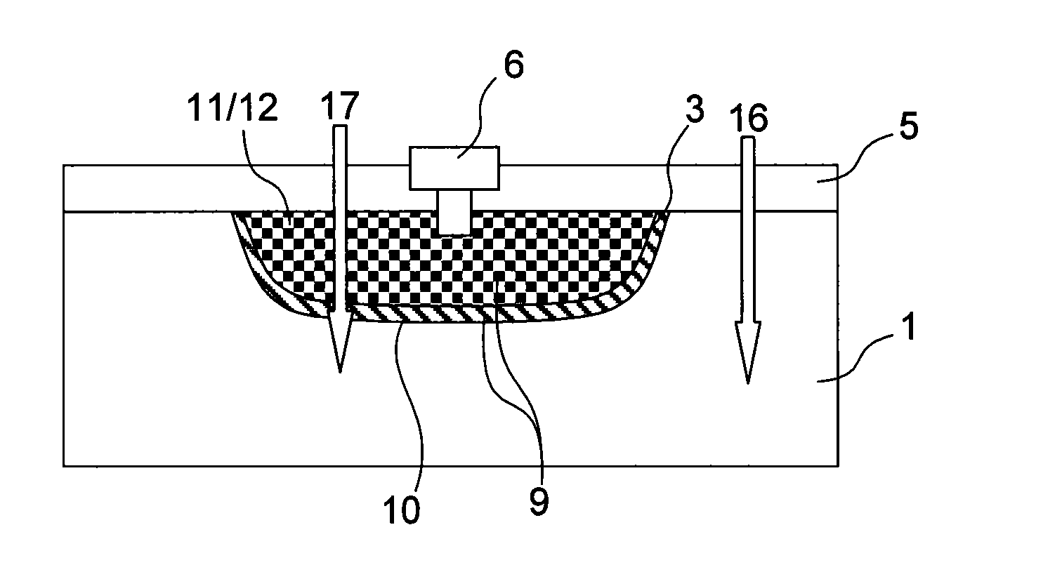
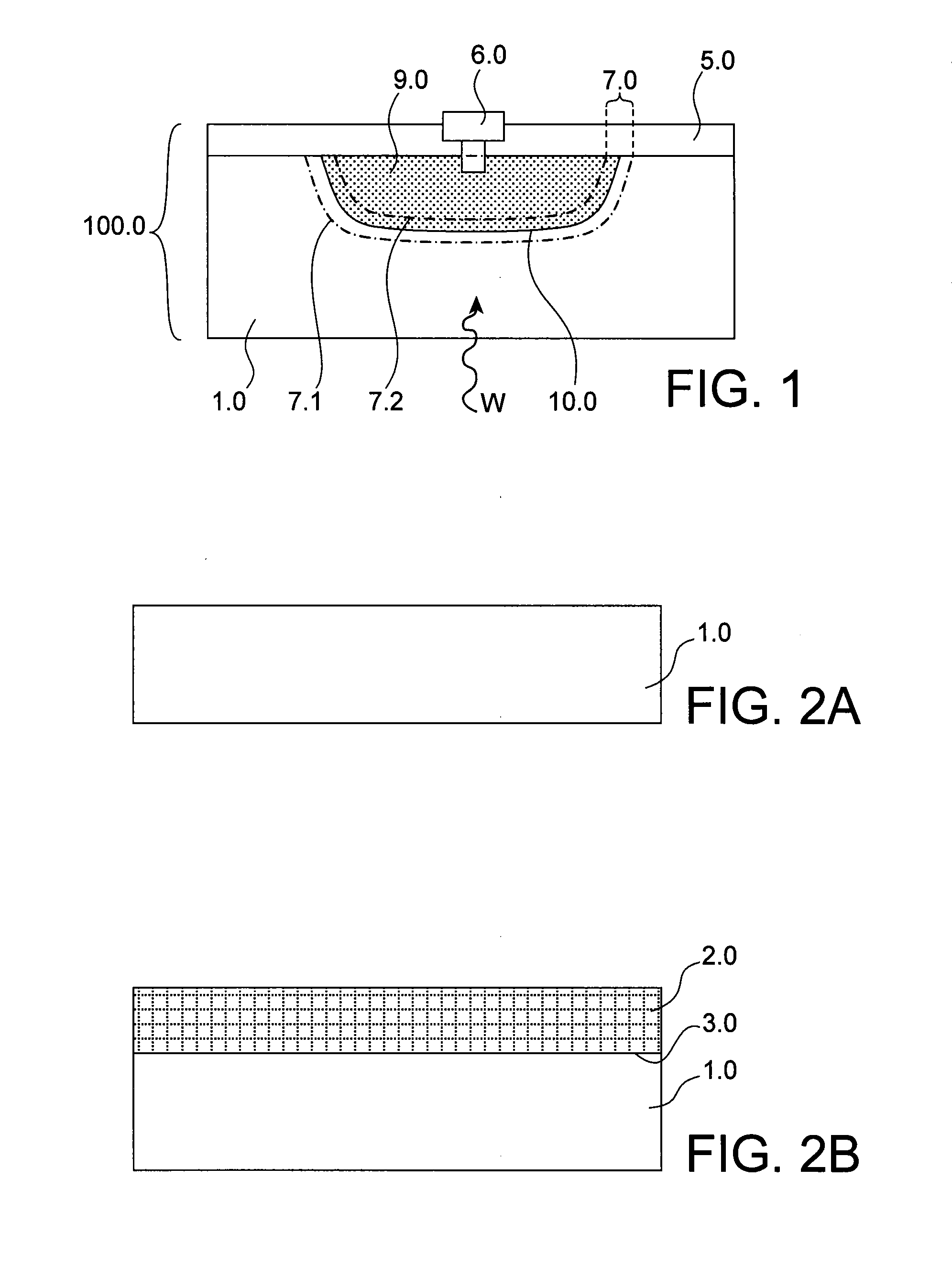
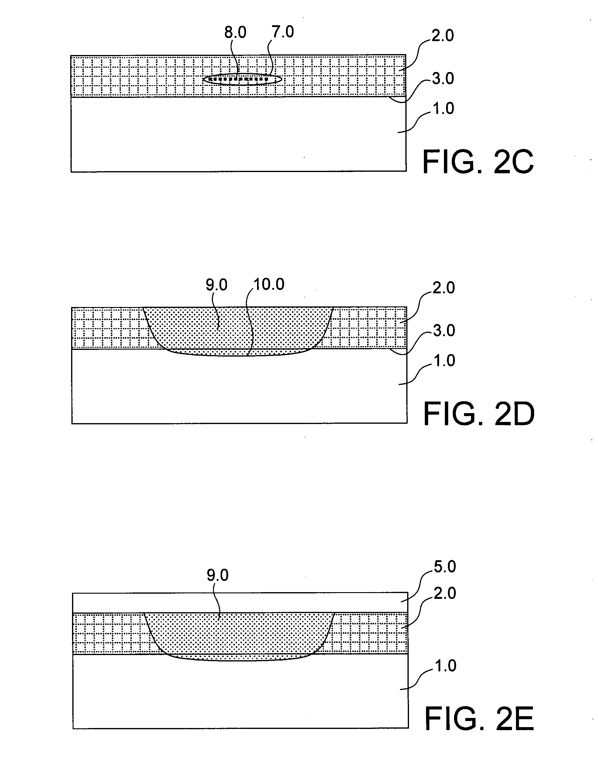
[0034]The invention thus firstly relates to a device having at least one heterostructure p / n diode, comprising a substrate based on Hg1-xCdxTe, mostly n-doped. The substrate comprises for each diode:[0035]a first part having a first cadmium concentration,[0036]a second part having a second cadmium concentration, greater than the first cadmium concentration, the second part, or concentrated part, forming a heterostructure with the first part,[0037]a p+ doped zon...


PUM


Abstract

A device including at least one heterostructure p/n diode, including a substrate based on HgCdTe including for each diode: a first part having a first cadmium concentration; a concentrated part, having a second cadmium concentration, greater than the first concentration, forming a heterostructure with the first part; a p+ doped zone situated in the concentrated part and extending into the first part, forming a p/n junction with an n-doped position of the first part, or a base plate; and the concentrated part is only located in the p+ doped zone and forms a substantially constant cadmium concentration well.

Description

FIELD OF THE INVENTION[0001]The present invention relates to the field of diodes manufactured in semiconductor materials. The invention relates more specifically to p / n type diodes formed in substrates based on Hg1-xCdxTe type materials, which may be used for infrared imagers.STATE OF THE RELATED ART[0002]P / N diodes are generally formed in a substrate 100.0 having mostly n doping. They comprise in this substrate 100.0 an n doping region, called the base plate 1.0 (FIG. 1) and a p+ doped zone 9.0, or p doping zone, adjacent to the base plate 1.0. The interface between the n doping region 1.0 and the p+ doped zone 9.0 is commonly referred to as the “p / n junction”10.0. At thermodynamic equilibrium, a space charge zone 7.0 is formed on either side of the p / n junction 10.0. At a first boundary 7.1 of the space charge zone 7.0, the n-doped base plate 1.0 is positively charged and at a second boundary 7.2 of the space charge zone, the p+ doped zone 9.0 is negatively charged inducing an int...

Claims


Application Information

Patent Timeline
IPC IPC(8): H01L31/109H01L31/18H01L31/0296
CPCH01L31/109H01L31/1832H01L31/02966H01L31/1032
Inventor MOLLARD, LAURENTBAIER, NICOLASROTHMAN, JOHAN
Owner COMMISSARIAT A LENERGIE ATOMIQUE ET AUX ENERGIES ALTERNATIVES
Why Eureka
Try Eureka