Radiometer and method for use of same
a technology of radiometer and esr, which is applied in the direction of optical radiation measurement, discharge tube/lamp details, instruments, etc., can solve the problems of many esrs being bulky and the time response of many esrs not optimal for detecting transient optical signatures
- Summary
- Abstract
- Description
- Claims
- Application Information
AI Technical Summary
Benefits of technology
Problems solved by technology
Method used
Image
Examples
example 1
First Radiometer
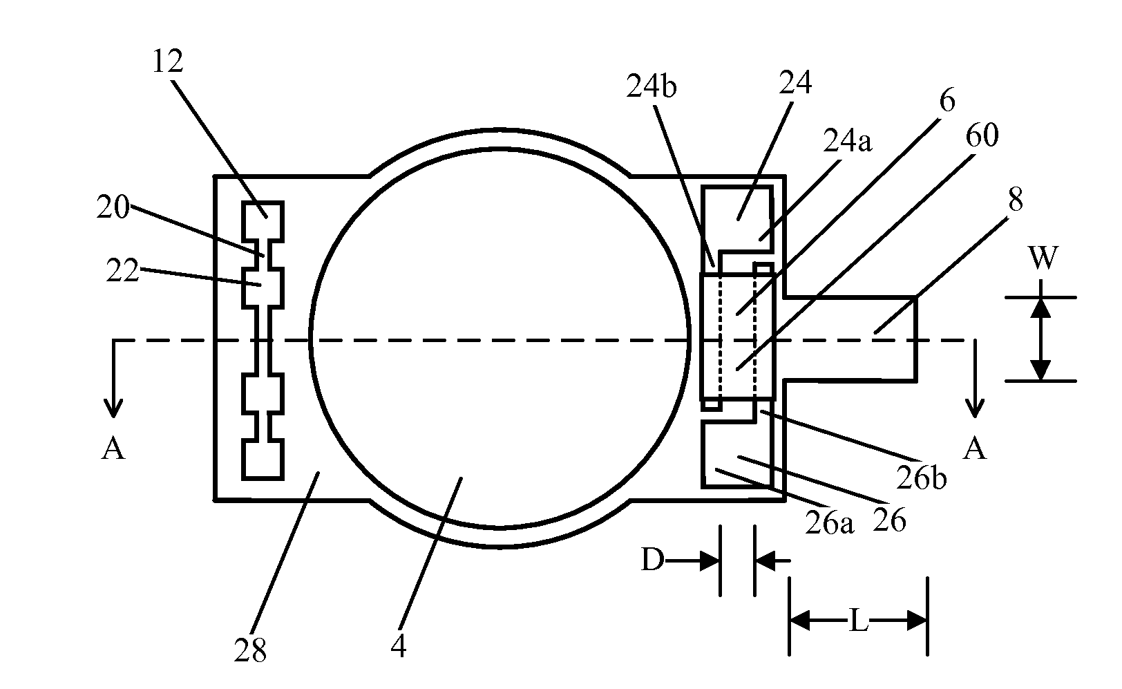
[0121]A radiometer was made as described in Tomlin et al., Optics Letters 38, 175 (2013), the disclosure of which is incorporated by reference herein in its entirety. With reference to FIGS. 31A, 31B, and 31C, radiometer 101 was fabricated from a double-side polished silicon wafer, which was lithographically patterned and micromachined using a Bosch process plasma etch to define the geometry (FIG. 31A). The silicon leg that sets thermal link 108 had dimensions of 6.7 mm long, 2.6 mm wide, and 375 nm thick. VACNTs were grown by first depositing 500 nm of SiO2 and 20 nm Al followed by oxidizing the Al to Al2O3 and depositing 2 nm Fe, and then chemical vapor deposition nanotube growth at 750° C. for 2.5 min. The VACNTs were 150 μm long and grown in 9 mm circles from use of a shadow mask during Fe deposition as shown in FIG. 31B. A second shadow mask was used to deposit 34 nm of Au at opposite sides of each VACNT region. Electrical contact was made to each VACNT region v...
example 2
Second Radiometer
[0123]A second radiometer was made using a shadowmask wafer and lithographic fabrication on a 76.2 mm diameter silicon wafer. A molybdenum thin film was disposed on the silicon wafer and subjected to wet etching followed by formation of Al2O3 and Fe with micro-machined silicon etch, and VACNT growth. A scanning electron microscope (SEM) micrograph of the resulting radiometer from the shadowmask wafer is shown in FIG. 32.
example 3
Third Radiometer
[0124]A third radiometer was made by lithographically fabrication on a 76.2 mm diameter silicon wafer. A molybdenum thin film was disposed on the silicon wafer and subjected to wet etching followed Al2O3 and Fe liftoff with micro-machined silicon etch, and VACNT growth. An SEM micrograph of the resulting radiometer from the liftoff wafer is shown in FIG. 33A. SEM micrographs of the VACNTs at various magnification are shown in FIGS. 33B, 33C, and 33D.
PUM
| Property | Measurement | Unit |
|---|---|---|
| wavelength | aaaaa | aaaaa |
| time constant | aaaaa | aaaaa |
| temperature | aaaaa | aaaaa |
Abstract
Description
Claims
Application Information


