
Semiconductor device

a semiconductor device and a technology of a semiconductor device, applied in the direction of semiconductor devices, basic electric elements, electrical appliances, etc., can solve the problems high turn-on resistance of semiconductor devices, and achieve the effect of slow channel formation speed, suppressing the increase in turn-on voltage, and high maximum voltag

Inactive Publication Date: 2014-11-27
TOYOTA JIDOSHA KK +1
View PDF1 Cites 3 Cited by
  • Summary
  • Abstract
  • Description
  • Claims
  • Application Information

AI Technical Summary

Benefits of technology

The patent text describes a MOSFET structure with a high maximum voltage and excellent turn-on characteristics. The technical effect of this structure is achieved through a combination of various insulating films and a specific arrangement of the gate electrode and semiconductor substrate. By increasing the thickness of the insulating film at the corner portion of the lower end of the gate electrode, dielectric breakdown can be prevented without impeding channel formation when the gate electrode is turned on. The use of insulating films with different dielectric constants and the arrangement of the gate electrode and semiconductor substrate can also help to slow down the speed of channel formation and enhance the efficiency of the MOSFET.

Problems solved by technology

However, if the insulating film at the corner portion of the lower end of the gate electrode is made thick, the insulating film of the trench side surface also becomes thick, whereby channel formation when the gate electrode is turned on is impeded, resulting in high turn-on resistance of the semiconductor device.
Further, if the third insulating film with a high dielectric constant is in contact with the semiconductor substrate, many carriers are captured at an interface state at the interface between the third insulating film and the semiconductor substrate, and the speed of channel formation may become slow.

Method used


Image

  • Semiconductor device
  • Semiconductor device

Examples


example 1

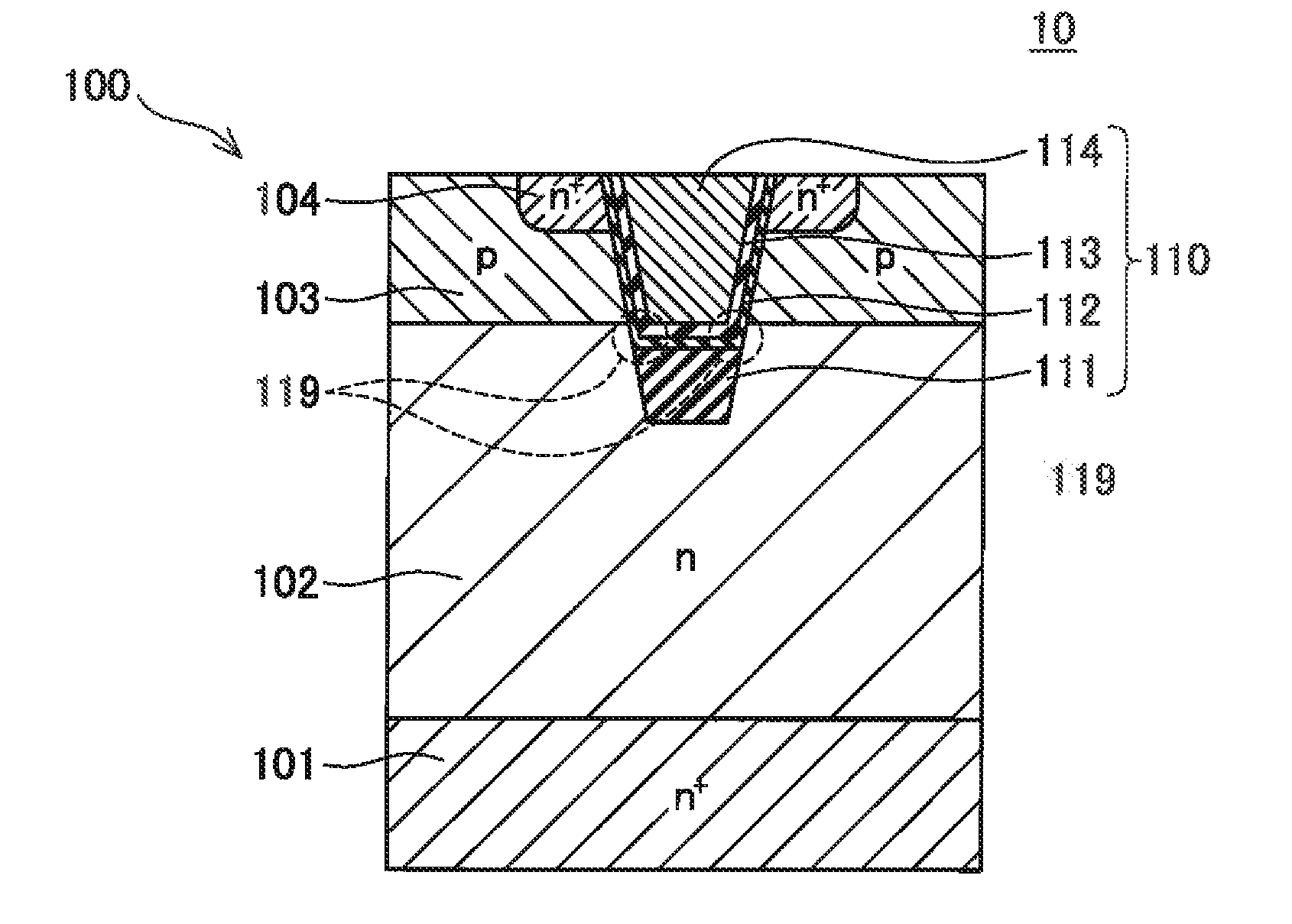
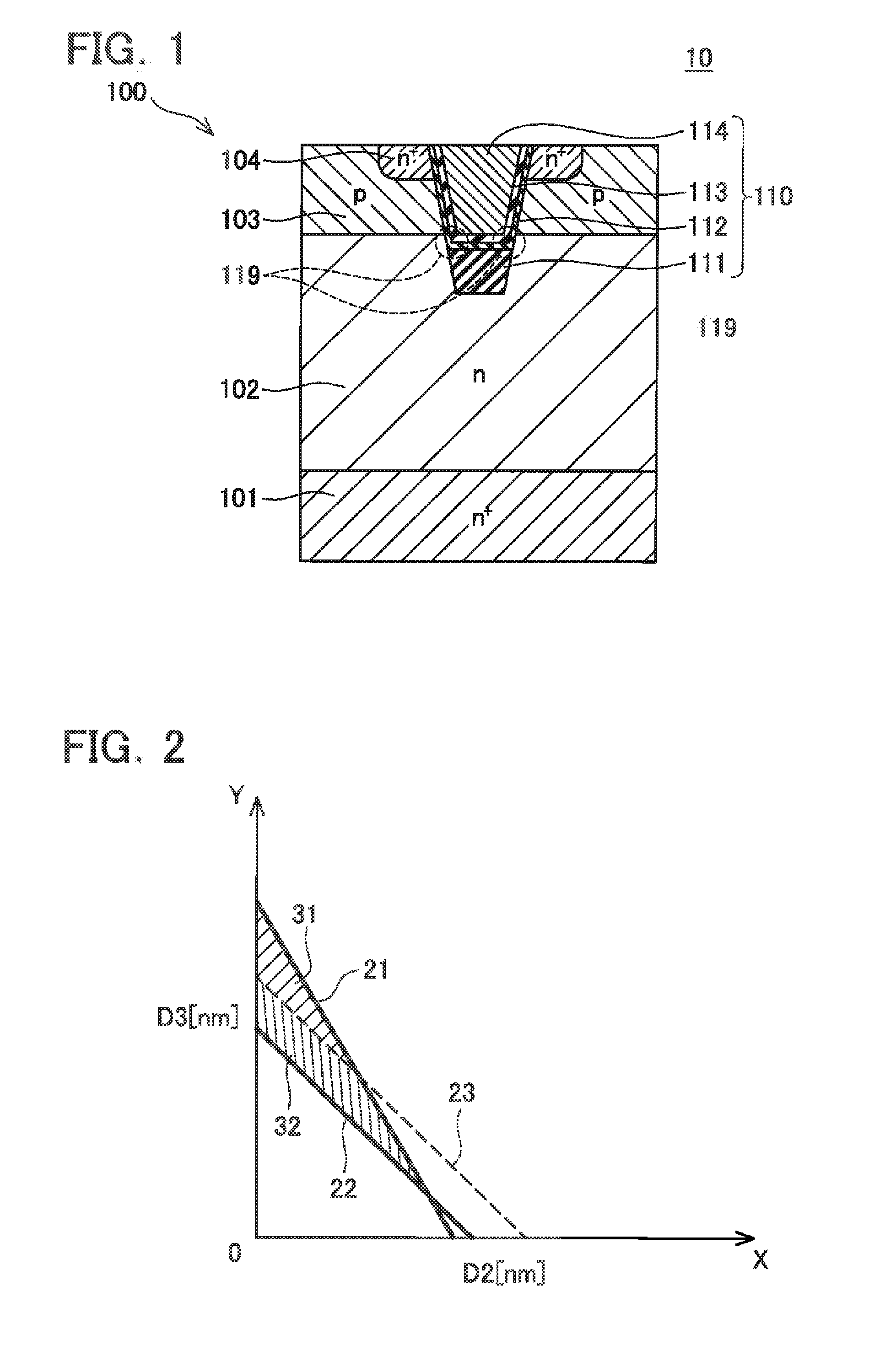
[0020]As shown in FIG. 1, a MOSFET 10 of Embodiment 1 comprises a semiconductor substrate 100 and a trench gate 110. Material of the semiconductor substrate 100 is silicon carbide. The semiconductor substrate 100 comprises an n+ type drain layer 101; n type drift layer 102 formed on a surface of the drain layer 101; p type body layer 103 formed on a surface of the drift layer 102; and n+ type source layer 104 formed on a part of a surface of the body layer 103. The drain layer 101 is exposed at a rear surface of the semiconductor substrate 100, and is in contact with a rear surface electrode (not shown). A part of the body layer 103 and the source layer 104 are exposed at a surface of the semiconductor substrate 100, and are in contact with a surface electrode (not shown). The trench gate 110 penetrates through the body layer 103 and the source layer 104 from the surface of the semiconductor substrate 100, and reaches the drift layer 102. The trench gate 110 comprises a first insula...


PUM


Abstract

A vertical MOSFET includes: a semiconductor substrate comprising a drain layer, a drift layer, a body layer, and a source layer; and a trench gate penetrating through the source layer and the body layer from an upper surface of the semiconductor substrate and reaching the drift layer. The trench gate includes a gate electrode; a first insulating film disposed on a bottom surface of a trench formed in the semiconductor substrate; a second insulating film disposed at least on a side surface of the trench, and in contact with the body layer; and a third insulating film disposed between the gate electrode and the second insulating film, and formed of a material of which dielectric constant is higher than a dielectric constant of the second insulating film.

Description

TECHNICAL FIELDCross-Reference to Related Application[0001]This application claims priority to Japanese Patent Application No. 2011-270084 filed on Dec. 9, 2011, the contents of which are hereby incorporated by reference into the present application.[0002]The teaching herein relates a semiconductor device provided with a vertical MOSFET having a trench gate.BACKGROUND ART[0003]In Japanese Patent Application Publication No. 2005-223255, in order to raise a maximum voltage of a trench gate-type semiconductor device, a thick insulating film is formed on a bottom surface of a trench. Leakage current is suppressed by this thick insulating film, and the maximum voltage of the semiconductor device is raised.SUMMARY OF INVENTION[0004]In Japanese Patent Application Publication No. 2005-223255, a corner portion of a lower end of a gate electrode and a semiconductor substrate are separated by a comparatively thin insulating film that also serves as an insulating film on a trench surface side. ...

Claims


Application Information

Patent Timeline
Patent Type & Authority Applications(United States)
IPC IPC(8): H01L29/78H01L29/423H01L29/10H01L29/51
CPCH01L29/7813H01L29/1095H01L29/42368H01L29/512H01L29/513
Inventor SOENO, AKITAKAYAMAMOTO, TOSHIMASAWATANABE, YUKIHIKO
Owner TOYOTA JIDOSHA KK
Learn More