
Fault-tolerant power semiconductor switching device control system

a technology of switching device control and fault tolerance, which is applied in the direction of electronic switching, pulse generator, pulse technique, etc., can solve the problems of difficult to achieve and relatively common error in fault detection data bits, and achieve the effect of convenient rapid detection and rapid detection

Active Publication Date: 2014-11-27
MASCHFAB REINHAUSEN GEBR SCHEUBECK GMBH & CO KG
View PDF7 Cites 14 Cited by
  • Summary
  • Abstract
  • Description
  • Claims
  • Application Information

AI Technical Summary

Benefits of technology

The patent describes a system that uses intermediate states to create a fault-tolerant architecture. This means that if a fault is detected, the system can quickly control a device or set of devices into a safe state to prevent collateral damage. The system also merges and analyzes the data from the device controllers to quickly detect any errors or if the devices are in the required target state. This helps to limit collateral damage and take remedial action as quickly as possible.

Problems solved by technology

In theory the switching control data could be sent at times which avoid electrically noisy switching intervals, but in a large system this can be difficult to achieve and, instead, it has been found better to control using a ‘lockstep’ approach in which after a switching stage, further switching is dependent on the content of the acknowledgement data.
In a large switching control system in a noisy environment an error in a fault detection data bit may be relatively common.

Method used


Image

  • Fault-tolerant power semiconductor switching device control system
  • Fault-tolerant power semiconductor switching device control system
  • Fault-tolerant power semiconductor switching device control system

Examples


Embodiment Construction

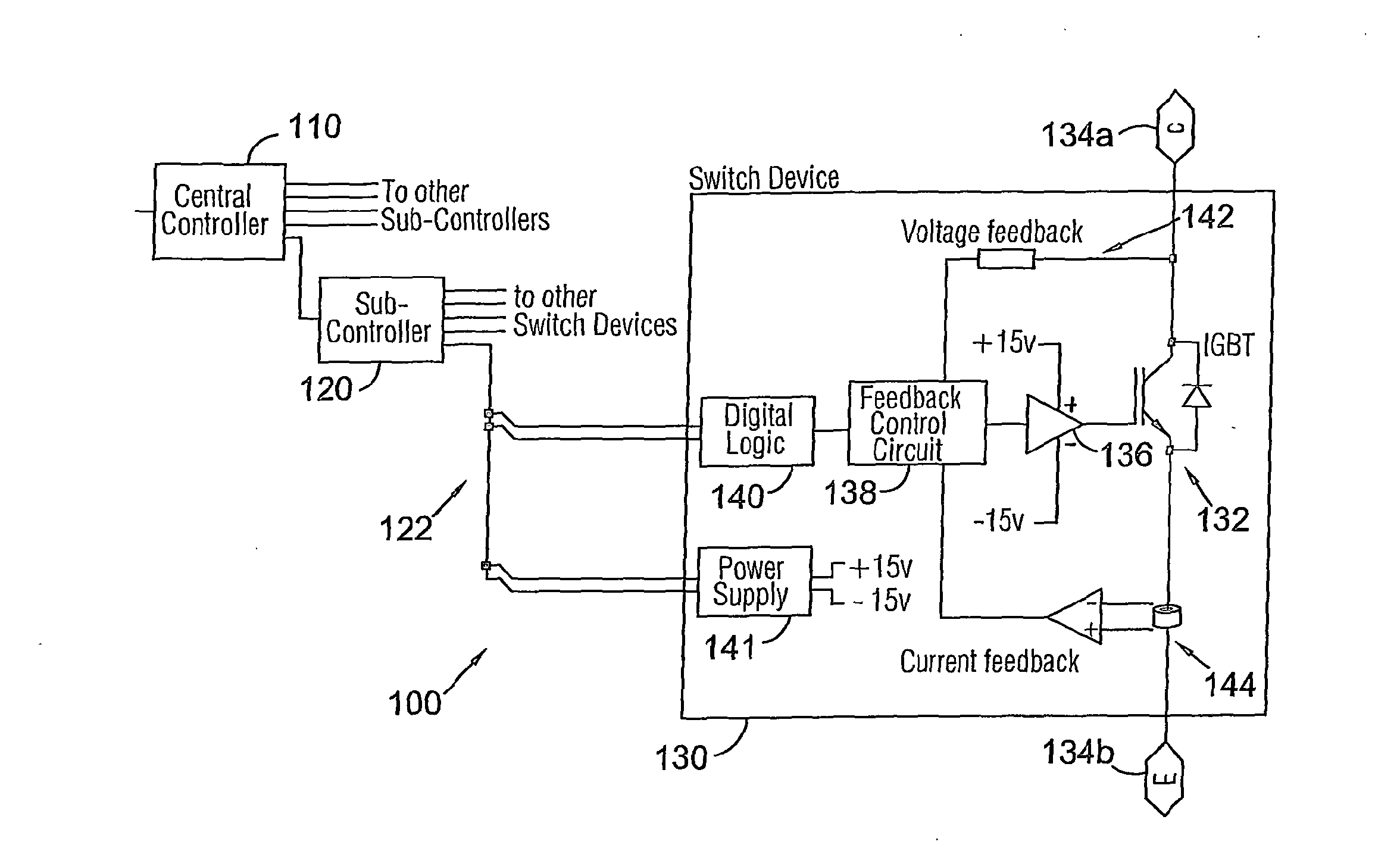
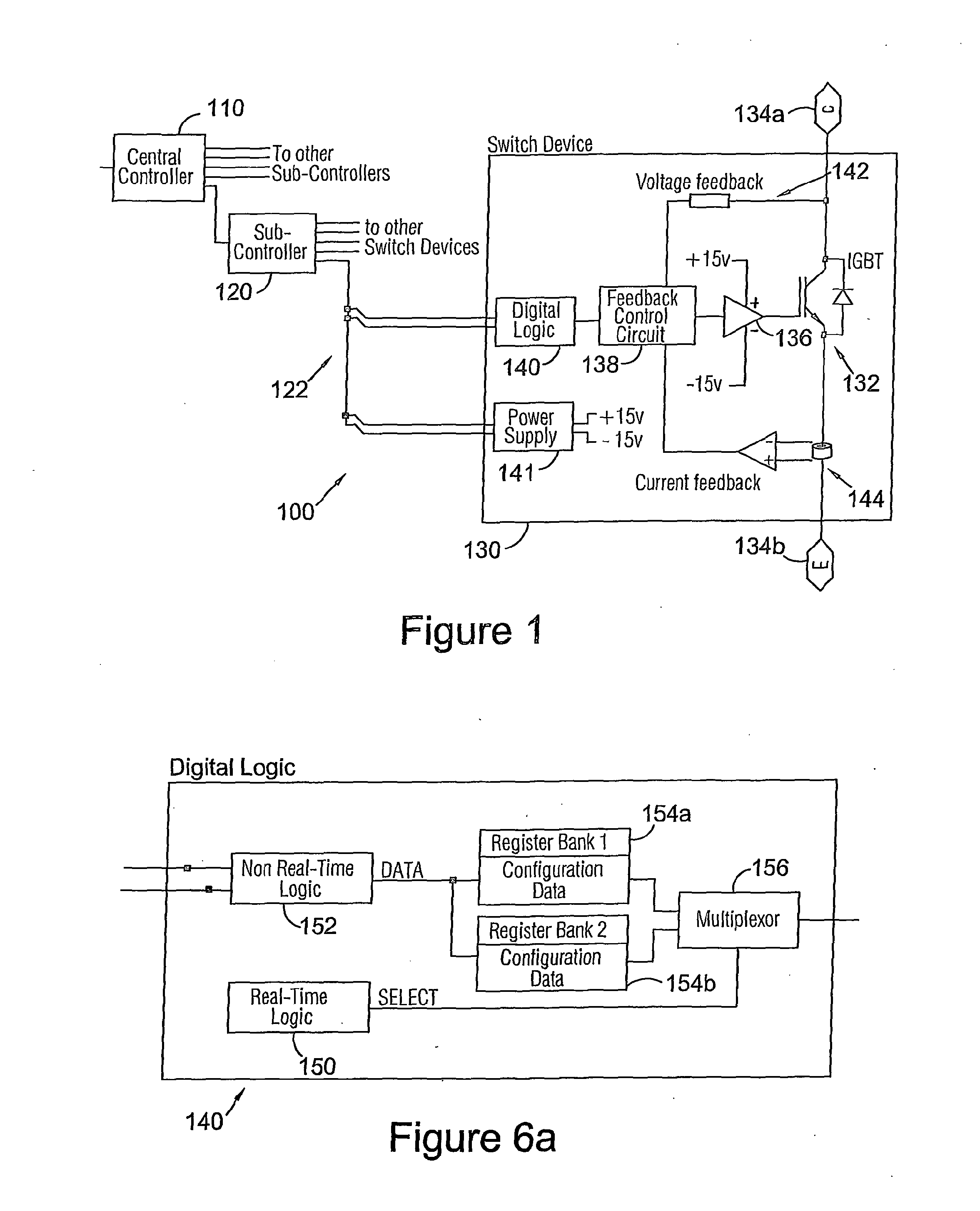
[0032]Referring to FIG. 1a, an embodiment of a power semiconductor switching device control system 100 comprises a central controller 110 coupled to a plurality of sub-controllers 120 of which one is illustrated, in turn coupled to a plurality of switching device controllers 130 (again just one is illustrated). In the following description the switching device controller 130 is sometimes referred to as a switch device (SD); and the central controller and sub-controller are sometimes abbreviated to CC and SC respectively. Although in the example of FIG. 1a a sub-controller is provided, this is not essential and embodiments of the control system may employ just a central controller. Other embodiments of the control system may employ multiple levels of (nested) sub-controllers.

[0033]A power electronics system or circuit generally comprises a plurality of switches each of which may comprise one, or typically multiple switching devices.

[0034]In the example of FIG. 1a the power semiconduc...


PUM


Abstract

We describe a fault-tolerant power semiconductor switching device control system (100), the control system comprising: a coordinating control system (110); and a plurality of switching device controllers (120) each coupled to said coordinating control system and each configured to control a respective power semiconductor switching device (130); wherein said coordinating control system is configured to send real time switching control data to said switching device controllers to control switching of said power semiconductor switching devices, and to receive real time acknowledgement data from said switching device controllers; wherein a said switching device controller is configured to receive said real time switching control data from said coordinating control system, to control a said power semiconductor switching device responsive to said real time switching control data, and to provide said real time acknowledgement data confirming said switching device control to said coordinating control system; and wherein said coordinating control system is further configured to control further switching of said power semiconductor switching devices responsive to said real time acknowledgement data.

Description

FIELD OF THE INVENTION[0001]This invention relates to fault-tolerant systems and methods for controlling power semiconductor switching devices.BACKGROUND TO THE INVENTION[0002]The power semiconductor switching devices with which we are concerned typically have a current carrying capability of greater than 1 amp and are operable with a voltage of greater than 100 volts. Embodiments of the devices with which we are concerned are able to carry currents of greater than 10 amps, 50 amps or 100 amps and / or are able to sustain a voltage difference across the device of greater than 500 volts or 1 KV.[0003]Examples of such devices include insulated gate bipolar transistors (IGBTs), as well as FETs such as MOSFETS (vertical or lateral) and JFETs, and potentially devices such as LILETs (lateral inversion layer emitter transistors), SCRs and the like. The techniques we will describe are not limited to any particular type of device architecture and thus the power switching devices may be, for ex...

Claims


Application Information

Patent Timeline
IPC IPC(8): H03K17/082G01R31/327
CPCG01R31/327H03K17/0822H03K17/0828H03K17/18H02M1/325H02M1/08H02M1/32H03K17/08126H03K17/0826H03K17/08122H01H83/10H01H83/06H01H83/20
Inventor SNOOK, MARKSHELTON, EDWARDPARKER, STEPHENVIT, MATTEO
Owner MASCHFAB REINHAUSEN GEBR SCHEUBECK GMBH & CO KG
Learn More