Arrangements with pyramidal features having at least one nanostructured surface and methods of making and using

Active Publication Date: 2014-12-04
WOSTEC
View PDF3 Cites 27 Cited by
  • Summary
  • Abstract
  • Description
  • Claims
  • Application Information

AI Technical Summary

Problems solved by technology

The larger junction surface area results in 1.7 times lager solar cell saturation current thus reducing cell efficiency.

Method used


Image

  • Arrangements with pyramidal features having at least one nanostructured surface and methods of making and using
  • Arrangements with pyramidal features having at least one nanostructured surface and methods of making and using
  • Arrangements with pyramidal features having at least one nanostructured surface and methods of making and using

Examples


Embodiment Construction

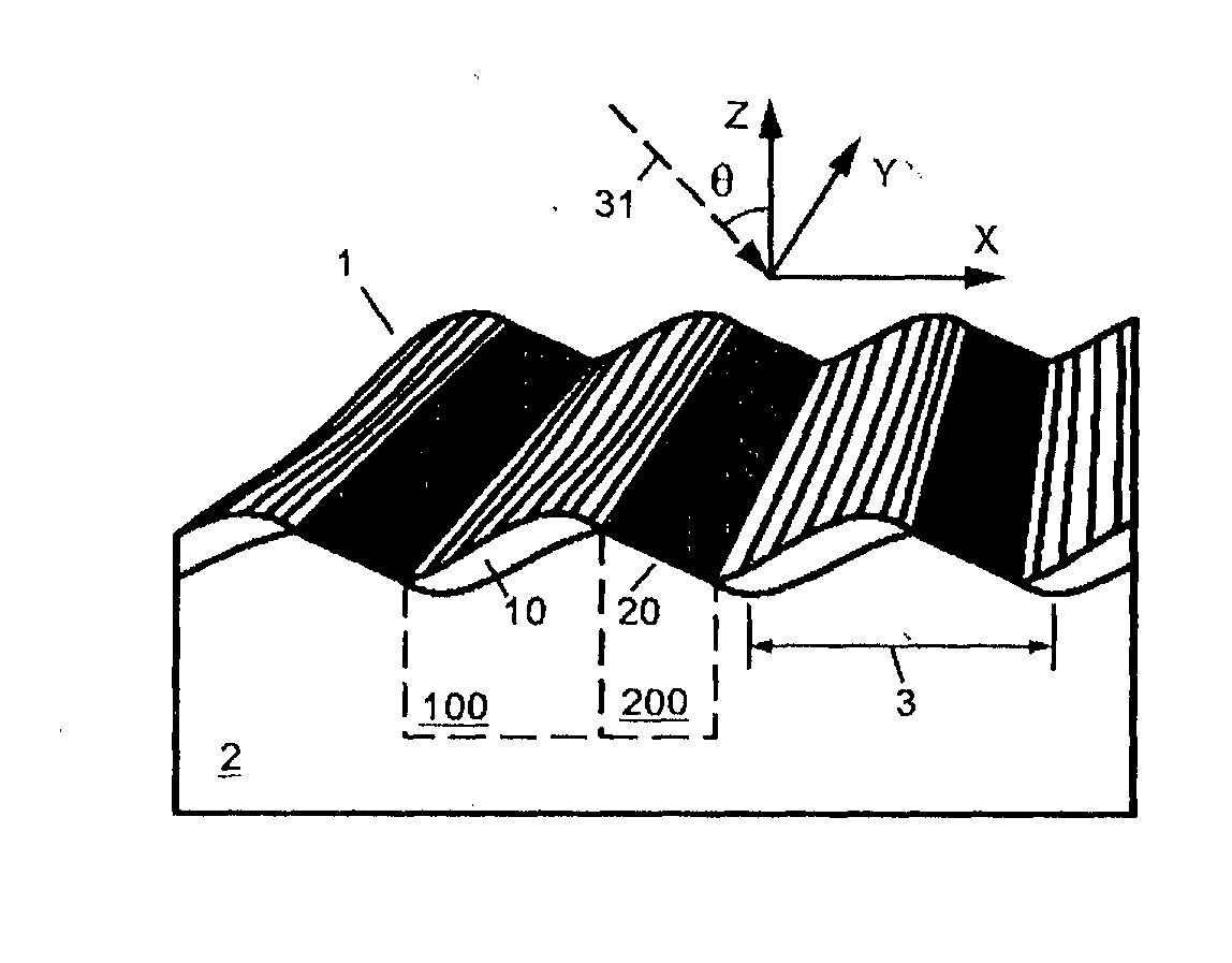
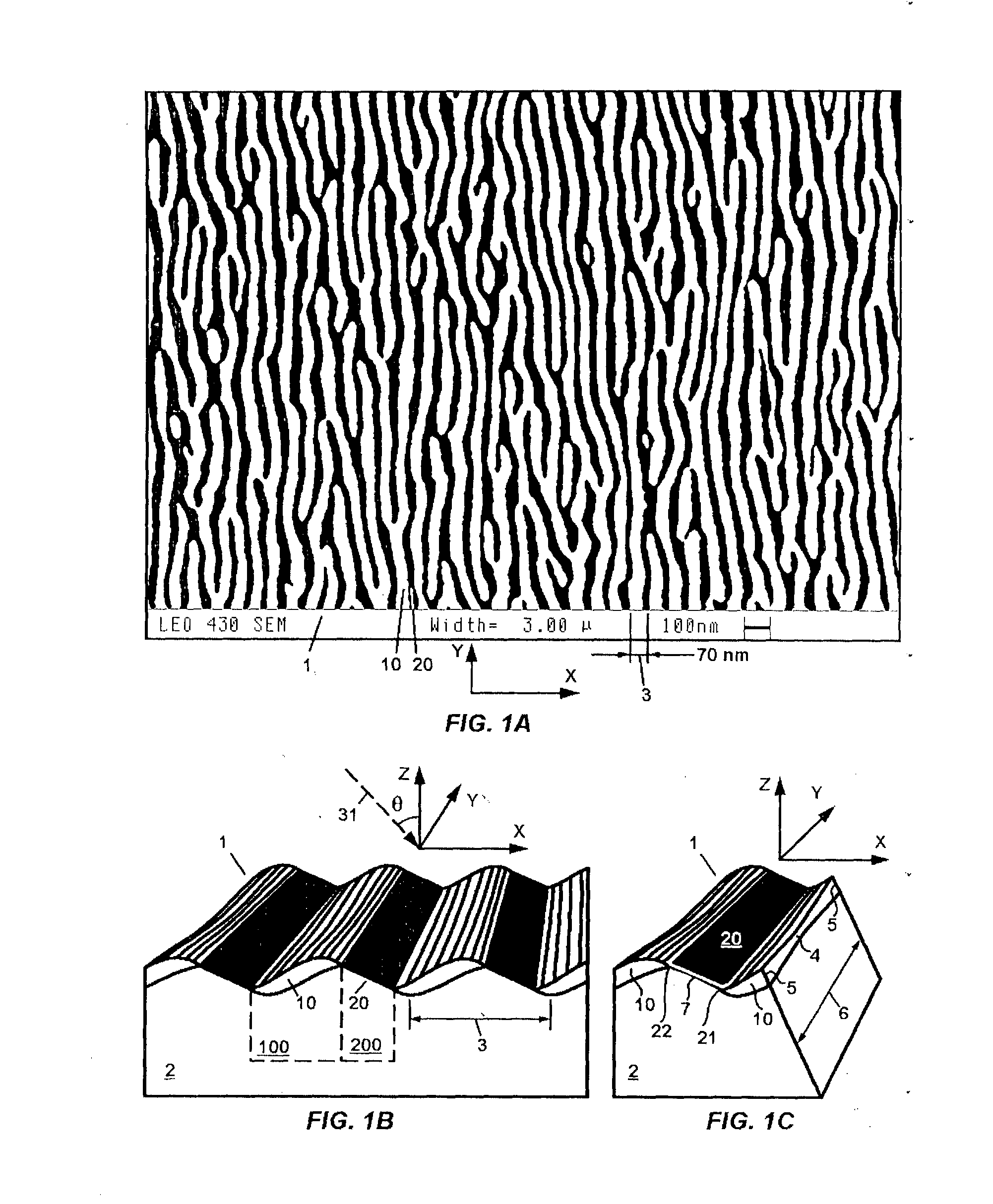
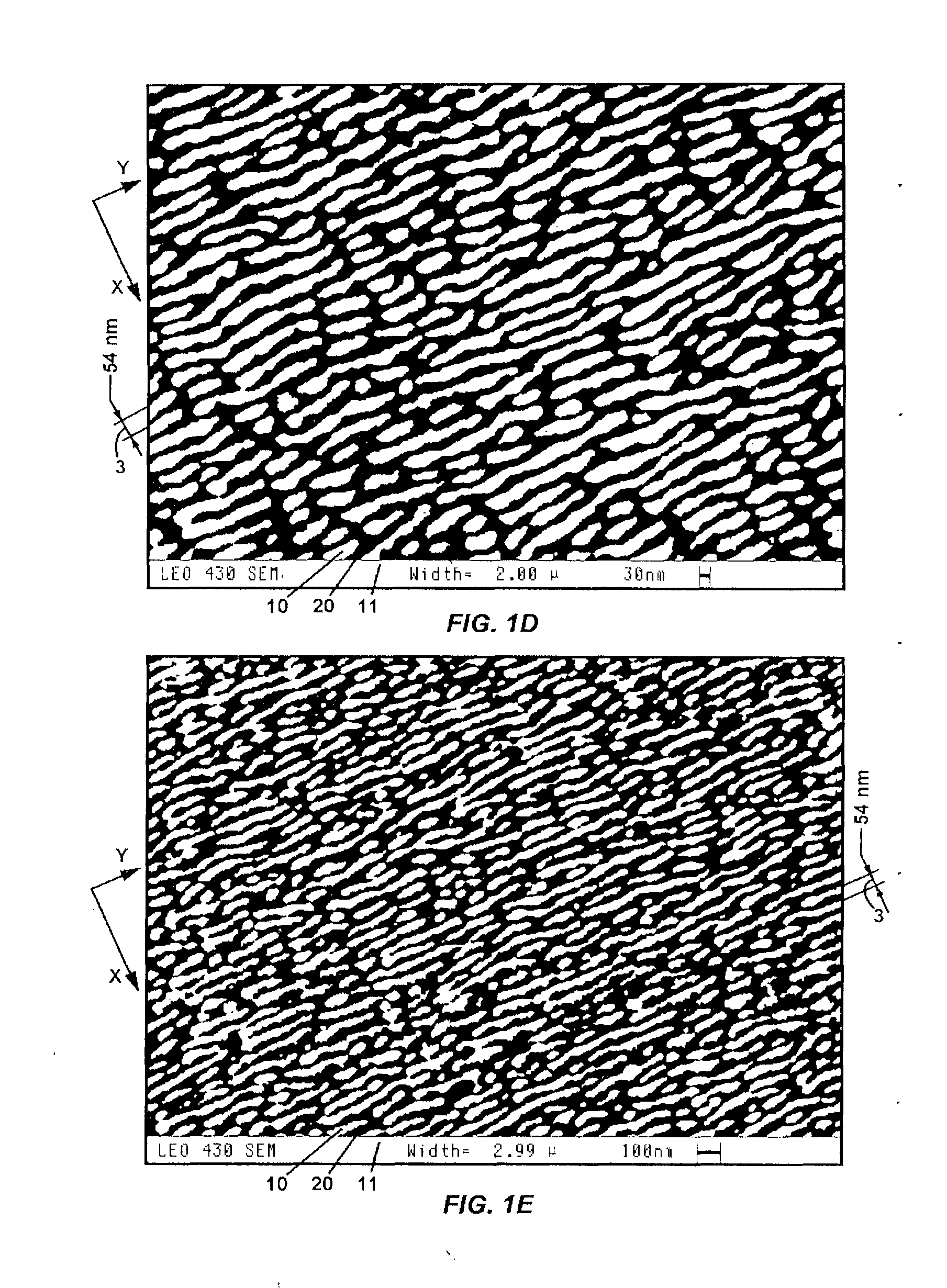
[0047]The invention relates to the field of arrangements with nanostructured surfaces and, in particular, arrangements with pyramidal features having one or more nanostructured surfaces. The invention also relates to the technology of forming nanostructured surfaces on pyramidal features. The invention also relates to the field of semiconductor devices for converting light energy into electric energy, in particular to the field of solar photovoltaic (PV) cells including cells based on monocrystalline and polycrystalline silicon. The invention also relates to the technology of forming nanostructured elements on the surface of silicon solar wafers to reduce the reflection of light from their surface.

[0048]A nanostructured arrangement can include a base with pyramidal features and at least one sloping nanostructured surface formed on at least one of the pyramidal features. The nanostructured arrangement can be used in a semiconductor device with, for example, the base and the pyramidal...


PUM


Abstract

One embodiment is a nanostructured arrangement having a base and pyramidal features formed on the base. Each pyramidal feature includes sloping sides converging at a vertex. The nanostructured arrangement further includes a nanostructured surface formed on at least one of the sloping sides of at least one of the pyramidal features. The nanostructured surface has a quasi-periodic, anisotropic array of elongated ridge elements having a wave-ordered structure pattern. Each ridge element has a wavelike cross-section and oriented substantially in a first direction.

Description

FIELD[0001]The invention relates to the field of arrangements with nanostructured surfaces and, in particular, arrangements with pyramidal features having one or more nanostructured surfaces. The invention also relates to the technology of forming nanostructured surfaces on pyramidal features.BACKGROUND[0002]Semiconductor devices are ubiquitous. One example of a semiconductor device is a solar cell. There is a general interest in the manufacture and use of solar cells as an alternative method for energy creation. FIG. 15A illustrates one type of conventional selective emitter solar cell. This solar cell includes a silicon wafer 150a with a base region 151a of p-type conductivity, diffusion regions 162 of p+-type, a low doped emitter layer 153 of n-type, a thin antireflection layer 154 covering the emitter layer, highly doped diffusion regions 163 of n+-type (selective emitter), contacts 155 extending through the layer 154 to regions 163, a layer of silicon oxide 156 with openings to...

Claims


Application Information

Patent Timeline
IPC IPC(8): H01L31/0236H01L31/18
CPCH01L31/02363H01L31/18B82B1/005Y10S977/888B82B3/008Y10S977/948B82Y40/00B82B3/0014B82Y30/00Y02E10/50
Inventor SMIRNOV, VALERY K.KIBALOV, DMITRY S.
Owner WOSTEC
Why Eureka
Try Eureka