Preparation method of surface-enhanced Raman scattering substrate

A surface-enhanced Raman and substrate technology, applied in the field of surface spectroscopy, can solve the problems of complex process, harsh substrate requirements, unsuitable substrates, etc., to achieve the effect of reducing costs, mild imprinting conditions, and saving raw materials

Inactive Publication Date: 2013-05-08
NANJING FENGQIANG NANO TECH
View PDF5 Cites 23 Cited by
  • Summary
  • Abstract
  • Description
  • Claims
  • Application Information

AI Technical Summary

Problems solved by technology

However, the preparation of SERS substrates using traditional nanoimprinting technology is extremely demanding on the substrate, requiring the substrate to be a rigid, planar template, which is not suitable for substrates with complex...

Method used


Image

  • Preparation method of surface-enhanced Raman scattering substrate
  • Preparation method of surface-enhanced Raman scattering substrate

Examples


preparation example Construction

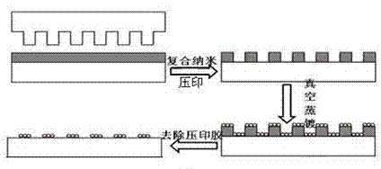
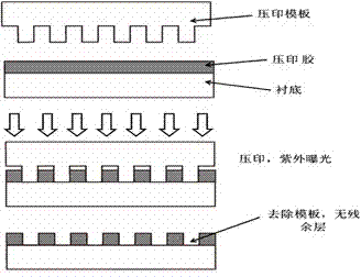
[0021] A method for preparing a surface-enhanced Raman scattering substrate, comprising the steps of:

[0022] 1. Prepare a flexible nanoimprint template with a double-layer composite structure with a pattern: the upper layer of the double-layer composite template is a flexible polymer elastomer substrate, and the Young's modulus ranges from 1 to 5 N / mm 2 , the lower layer is a rigid light-cured polymer imprint layer with a Young's modulus in the range of 20 N / mm 2 Above, its thickness is 20-500 nm, and the upper and lower layers are tightly bonded by bonding or chemical bonds; the lower layer is a rigid photocurable polymer imprint layer, and its surface is bonded with a layer of low surface energy fluorinated organic small molecules or polymer anti-corrosion sticky layer.

[0023] 2. Embossing ordered nanostructure patterns: using a composite nanoimprinting method to imprint ordered nanostructure patterns on the cleaned substrate surface with a flexible nanoimprint template...

Embodiment 1

[0029] A silicon wafer was selected as the substrate, and a layer of 500 nm multifunctional acrylate prepolymer was spin-coated on the surface of the cleaned 1 cm×1 cm substrate as a UV-curable nanoimprint adhesive, and the flexible nanoimprint template (as dots Array structure, the size of each groove is 800 nm×800 nm, and the pitch is 1 μm) to press the imprinting glue, so that the raised part of the imprinting template is in direct contact with the bottom of the substrate, and the template is removed after the imprinting glue is finalized , that is, an ordered lattice structure was built on a silicon wafer substrate by using a composite nanoimprint method, a layer of gold particles with a thickness of 50 nm was evaporated on the substrate, and finally O 2 The reactive ion etching process removed the barrier layer of the nanoimprint adhesive, thereby obtaining a uniformly distributed gold particle lattice with a pitch of 800 nm and a size of 1 μm×1 μm as the SERS substrate.


PUM

PropertyMeasurementUnit
Young's modulusaaaaaaaaaa
Thicknessaaaaaaaaaa

Abstract

The invention discloses a preparation method of a surface-enhanced Raman scattering substrate. The preparation method comprises the following steps of: (1) preparing a flexible nano imprinting template with patterns and in a double-layer composite structure; (2) imprinting ordered nano structure patterns; (3) carrying out vacuum evaporation; and (4) eliminating a nano imprinting gel baffle layer. The preparation method can be applied to preparation of all surface-enhanced Raman scattering substrates; the defects that the substrate is strictly required in preparing the SERS (Surface-Enhanced Raman Scattering) substrate in the conventional nano imprinting mode, and metal ordered structure SERS substrates with high resolution are hard to be prepared on complex appearance and high-curvature surfaces are overcome; and moreover the method is simple in process, can be used for producing high-performance SERS substrates with large area, large scale and low cost, can solve the preparation requirements of the SERS substrates and can meet the present practical requirements well.

Description

technical field [0001] The invention relates to the technical field of surface spectroscopy, in particular to a method for preparing a surface-enhanced Raman scattering substrate with an ordered structure. Background technique [0002] Since Martin Fleischmann first discovered the Surface Enhanced Raman scattering (SERS) phenomenon in the 1970s, after decades of development, SERS detection technology has been widely used in physics, chemistry, biology, medicine, materials, etc. In various fields, it has become an important tool for the trace detection of substance molecules. The preparation of active substrates is the prerequisite for obtaining SERS signals. In order to use SERS as a routine and online analysis tool, the prepared SERS substrates should have high signal enhancement ability and good uniformity, easy preparation and storage, and convenient use. At present, the methods used to prepare SERS active substrates mainly include sol-gel method, electrochemical dep...

Claims


Application Information

Patent Timeline
IPC IPC(8): G03F7/00
Inventor 潘革波李丰葛海雄
Owner NANJING FENGQIANG NANO TECH
Why Eureka
Try Eureka