
Oxygen precipitation in heavily doped silicon wafers sliced from ingots grown by the czochralski method

a technology of oxygen precipitation and silicon wafers, which is applied in the direction of basic electric elements, electrical apparatus, and semiconductor devices, etc., can solve the problems of affecting the operation of devices, contaminating molten silicon with various impurities, and precipitating harmful or beneficial effects

Active Publication Date: 2014-12-11
GLOBALWAFERS CO LTD
View PDF5 Cites 16 Cited by
  • Summary
  • Abstract
  • Description
  • Claims
  • Application Information

AI Technical Summary

Benefits of technology

The present invention relates to a method for controlling oxygen precipitation in a single crystal silicon wafer. The method involves heating the wafer at a specific temperature and for a specific duration to precipitate oxygen precipitates at a certain concentration. The resulting wafer should have no region with lower oxygen precipitate concentration. The invention also includes the use of specific dopants such as carbon, arsenic, and antimony to enhance the oxygen precipitation process. The technical effect of this invention is to improve the quality and reliability of single crystal silicon wafers for use in various electronic applications.

Problems solved by technology

Molten silicon is contaminated with various impurities, among which is mainly oxygen, during the time it is contained in a quartz crucible.
Depending upon their location in the wafer, the precipitates can be harmful or beneficial.
Oxygen precipitates located in the active device region of the wafer can impair the operation of the device.

Method used


Image

  • Oxygen precipitation in heavily doped silicon wafers sliced from ingots grown by the czochralski method
  • Oxygen precipitation in heavily doped silicon wafers sliced from ingots grown by the czochralski method
  • Oxygen precipitation in heavily doped silicon wafers sliced from ingots grown by the czochralski method

Examples


example 1

Segregation of Arsenic and Antimony in Boron-Doped Silicon Wafers

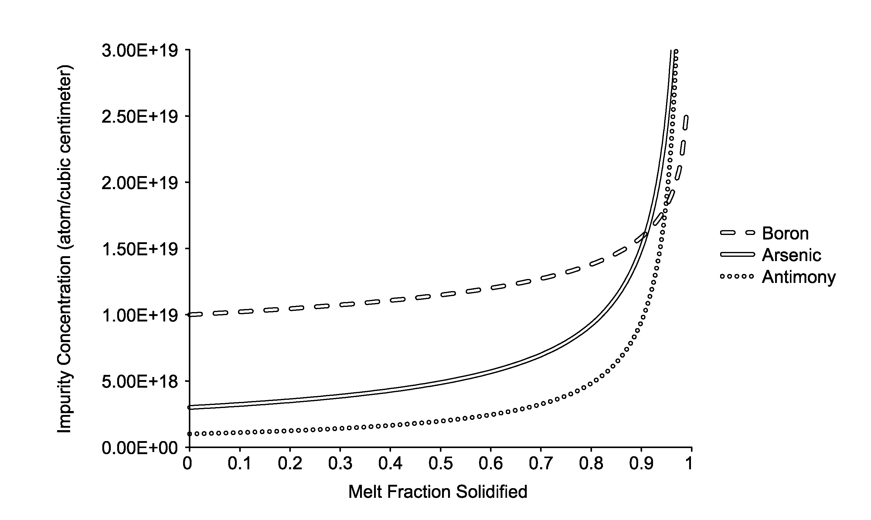
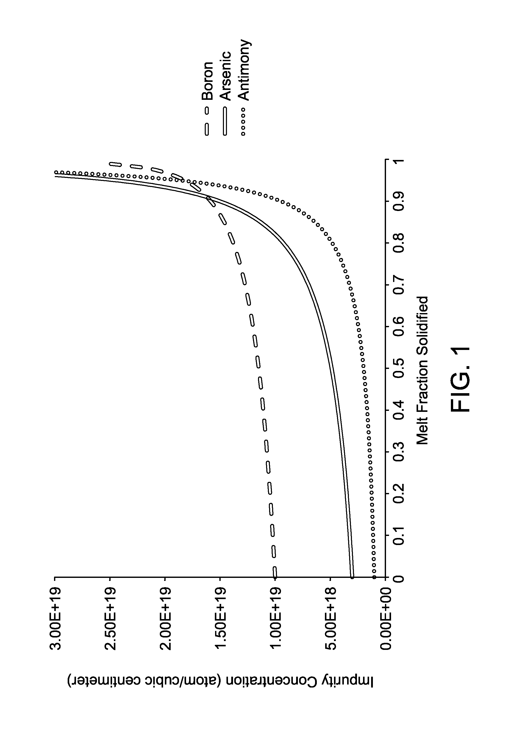
[0058]Highly boron doped single crystal silicon ingots are grown from a silicon melt by the Czochralski method. The ingots are doped with an additional dopant, arsenic or antimony. FIG. 1 is a graph depicting the expected boron, arsenic, and antimony concentrations as a fraction of the melt solidified. The data presented in the chart of FIG. 1 was obtained using the following calculation:

C(X)=C0*(1−X)(kseg-1)

wherein:

[0059]C(X) is the dopant concentration at a point along the constant diameter portion of the ingot;

[0060]C0 is the initial dopant concentration at the beginning of the constant diameter portion of the ingot;

[0061]X is the fraction of the ingot that is frozen;

[0062]kseg is the segregation coefficient.

[0063]Since boron has a segregation coefficient of 0.80, the concentration of boron as a function of the fraction of the melt solidified is relatively constant throughout most of the ingot growth. As can be see...


PUM


Abstract

A method for controlling oxygen precipitation in a single crystal silicon wafer having a wafer resistivity of less than about 10 milliohm-cm is provided so that the wafer has uniformly high oxygen precipitation behavior from the central axis to the circumferential edge. The single crystal silicon wafer comprises an additional dopant selected from among carbon, arsenic, and antimony.

Description

THE FIELD OF THE INVENTION[0001]The present invention generally relates to a method for the control of oxygen precipitation behavior in low resistivity silicon wafers, and more specifically to a method of providing uniform oxygen precipitation in low resistivity silicon wafers sliced from Czochralski-grown silicon ingots.BACKGROUND OF THE INVENTION[0002]Single crystal silicon, which is the starting material for most processes for the fabrication of semiconductor electronic components, is commonly prepared with the so-called Czochralski (Cz) process wherein a single seed crystal is immersed into molten silicon and then grown by slow extraction. Molten silicon is contaminated with various impurities, among which is mainly oxygen, during the time it is contained in a quartz crucible. At the temperature of the silicon molten mass, oxygen comes into the crystal lattice until it reaches a concentration determined by the solubility of oxygen in silicon at the temperature of the molten mass...

Claims


Application Information

Patent Timeline
IPC IPC(8): H01L29/36H01L21/02H01L21/223
CPCH01L21/02694H01L21/223H01L29/36H01L21/3225H01L21/324H01L21/02002H01L21/78
Inventor FALSTER, ROBERT J.VORONKOV, VLADIMIR V.
Owner GLOBALWAFERS CO LTD
Learn More