High-accuracy flat touch display panel structure

a touch display panel and high-accuracy technology, applied in non-linear optics, instruments, thermoelectric devices, etc., can solve the problems of increasing the additional weight and thickness increasing the reflectance and haze of the touch display panel, and reducing the light penetration rate. , to achieve the effect of increasing the linearity of the touch, reducing the gap distance between the touch sensor and the measurement of the dead area

Active Publication Date: 2014-12-18
SUPERC TOUCH CORP
View PDF1 Cites 7 Cited by
  • Summary
  • Abstract
  • Description
  • Claims
  • Application Information

AI Technical Summary

Benefits of technology

[0009]The object of the present invention is to provide a high-accuracy flat touch display panel structure, in which a plurality of wiring segments arranged in the first direction and a plurality of wiring segments arranged in the second direction are formed on a thin film transistor and wiring layer, such that there is no need to arrange wirings on a sensing electrode layer, so as to effectively reduce the gap distance between sensing touch patterns thereby decreasing the measure of dead area and increasing sensing linearity and sensing accuracy.

Problems solved by technology

Such well known skill of the touch panel may increase additional weight and thickness of the touch display panel, and may further reduce the light penetration rate, and increase reflectance and haze of the touch display panel.
Such a structure suffers the disadvantages of high material cost and complicated manufacturing process.
The structure of FIG. 3 has the advantages of low material cost and simplified manufacturing process; however, it suffers the disadvantage of complicated wirings 41.
Because the wirings 41 occupy most of the area, the linearity becomes unsatisfactory.

Method used


Image

  • High-accuracy flat touch display panel structure
  • High-accuracy flat touch display panel structure
  • High-accuracy flat touch display panel structure

Examples


Embodiment Construction

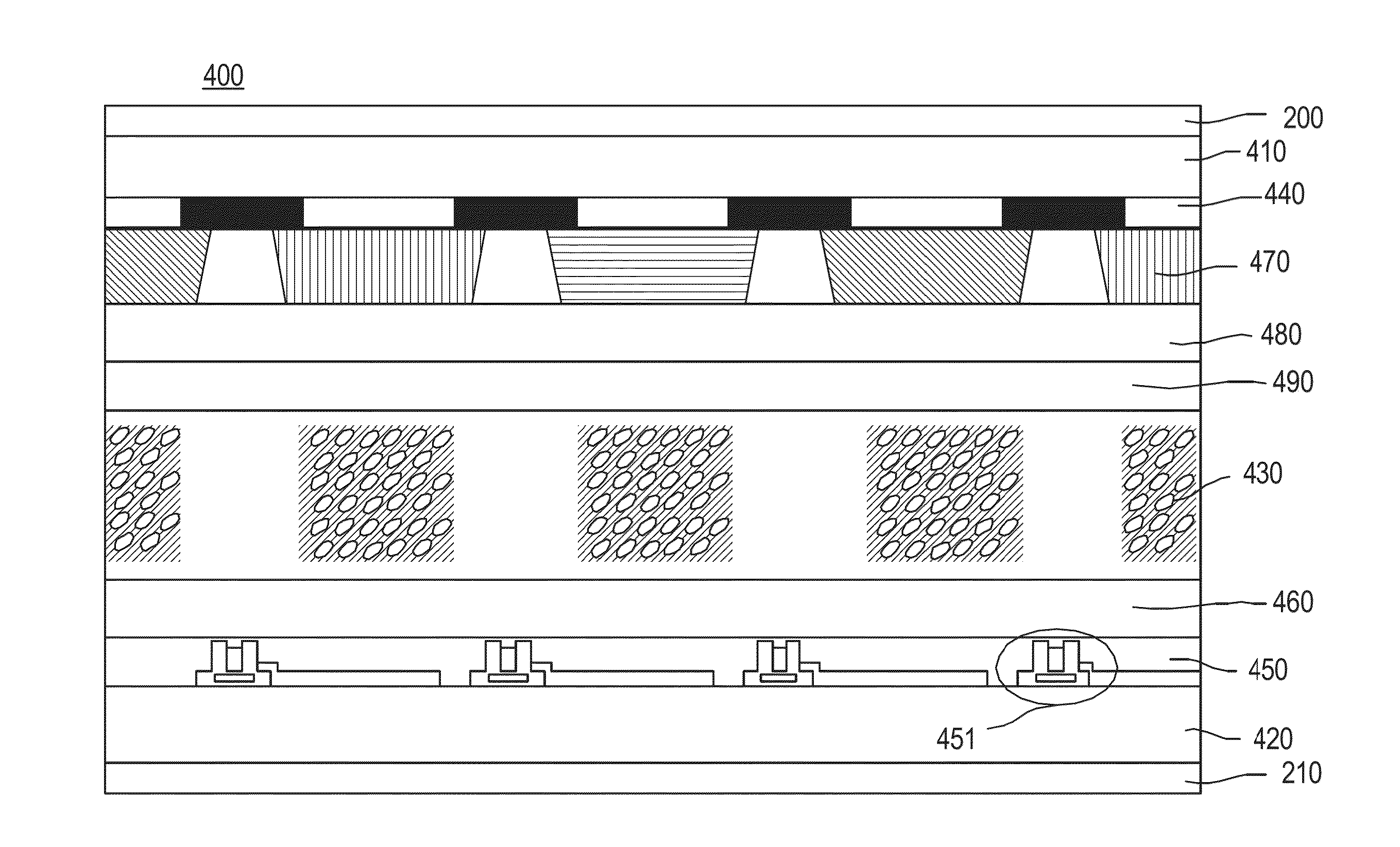
[0028]The present invention relates to a high-accuracy flat touch display panel structure. FIG. 4 is a schematic diagram of the high-accuracy flat touch display panel structure in accordance with an embodiment of the present invention. As shown, the high-accuracy flat touch display panel structure 400 includes an upper substrate 410, a lower substrate 420, a liquid crystal layer 430, a black matrix layer 440, a thin film transistor and wiring layer 450, a sensing electrode layer 460, a color filter layer 470, an over coat layer 480, a common electrode layer (Vcom) 490, a first polarizer layer 200 and a second polarizer layer 210.

[0029]The upper substrate 410 and the lower substrate 420 are preferably glass substrates, and are parallel to each other. The liquid crystal layer 430 is disposed between the upper and lower substrates 410, 420.

[0030]The thin film transistor and wiring layer 450 is disposed at one side of lower substrate 420 that faces the liquid crystal layer 430. The thin...


PUM

PropertyMeasurementUnit
thicknessaaaaaaaaaa
weightaaaaaaaaaa
volumeaaaaaaaaaa

Abstract

A high-accuracy flat touch display panel structure includes an upper substrate, a lower substrate, a liquid crystal layer configured between the upper and lower substrates, a thin film transistor and wiring layer, and a sensing electrode layer. The thin film transistor and wiring layer is disposed at one side of the lower substrate facing the liquid crystal layer, and includes a plurality of gate lines, a plurality of source lines, and a plurality of wirings. The sensing electrode layer is disposed at one side of the thin film transistor and wiring layer facing the liquid crystal layer, and has a plurality of sensing conductor lines. The plurality of sensing conductor lines are disposed corresponding to positions of the plurality of gate lines and the plurality of source lines.

Description

BACKGROUND OF THE INVENTION[0001]1. Field of the Invention[0002]The present invention relates to a display screen structure with a touch panel and, more particularly, to a high-accuracy flat touch display panel structure.[0003]2. Description of Related Art[0004]In recent year, the flat panel display industry has been rapidly developed, and many products have also been made in pursuit of light weight, thinness, small volume and fine image quality for developing several types of flat-panel displays to replace traditional cathode ray tube display (CRT). FIG. 1 schematically illustrates the types of known display panels. As shown in FIG. 1, the flat panel display includes liquid crystal display (LCD), plasma display panel (PDP), organic light emitting diode (OLED) display, field emission display (FED), and vacuum fluorescence display (VFD).[0005]The conventional touch display panel includes a touch panel and a display unit overlapped with the touch panel. The touch panel is configured a...

Claims


Application Information

Patent Timeline
Patent Type & Authority Applications(United States)
IPC IPC(8): G06F3/041H01L27/32G02F1/1333
CPCG06F3/0412H01L27/323G02F1/13338G06F3/0443G06F3/0446G06F3/0448H10K59/40H10K50/15H10K50/16H10K59/38H10K59/131
Inventor LEE, HSIANG-YU
Owner SUPERC TOUCH CORP
Why Eureka
Try Eureka