Negative Audio Signal Voltage Protection Circuit and Method for Audio Ground Circuits

a technology for protecting circuits and negative audio signals, applied in the direction of circuit arrangements, emergency protective arrangements for limiting excess voltage/current, pulse techniques, etc., can solve problems such as introducing a large amount of distortion into the system, and achieve the effect of preventing distortion of output signals

Active Publication Date: 2014-12-18
TEXAS INSTR INC
View PDF5 Cites 8 Cited by
  • Summary
  • Abstract
  • Description
  • Claims
  • Application Information

AI Technical Summary

Benefits of technology

[0016]Is an object of the invention to provide improved audio ground switch circuitry that prevents buildup of charge and thereby prevents subsequent discharge thereof in depletion mode ground switch transistors under all operating conditions without compromising the quality of desired audio signals that are present.
[0017]It is another object of the invention to provide improved audio ground switch circuitry that prevents negative portions of an audio signal from causing ground switch circuitry receiving the audio signal to distort the audio signal.
[0018]Is another object of the invention to provide improved audio ground switch circuitry that prevents popping sounds caused by discharging of charge built up in the audio ground switch circuitry at the instant at which a headset is plugged into a jack receiving an audio signal.

Problems solved by technology

The resulting current through the headset speaker resistance may cause the above-mentioned clicking / popping sounds.
Unfortunately, if depletion mode transistor MP1 is switched into its high impedance OFF state, then the −0.8 volt portion of the AC signal VOUT1 on conductor 6-1 may cause parasitic diodes D2 and D3 to become forward biased, and that introduces a large amount of distortion into the system audio signal VOUT1.

Method used


Image

  • Negative Audio Signal Voltage Protection Circuit and Method for Audio Ground Circuits
  • Negative Audio Signal Voltage Protection Circuit and Method for Audio Ground Circuits
  • Negative Audio Signal Voltage Protection Circuit and Method for Audio Ground Circuits

Examples


Embodiment Construction

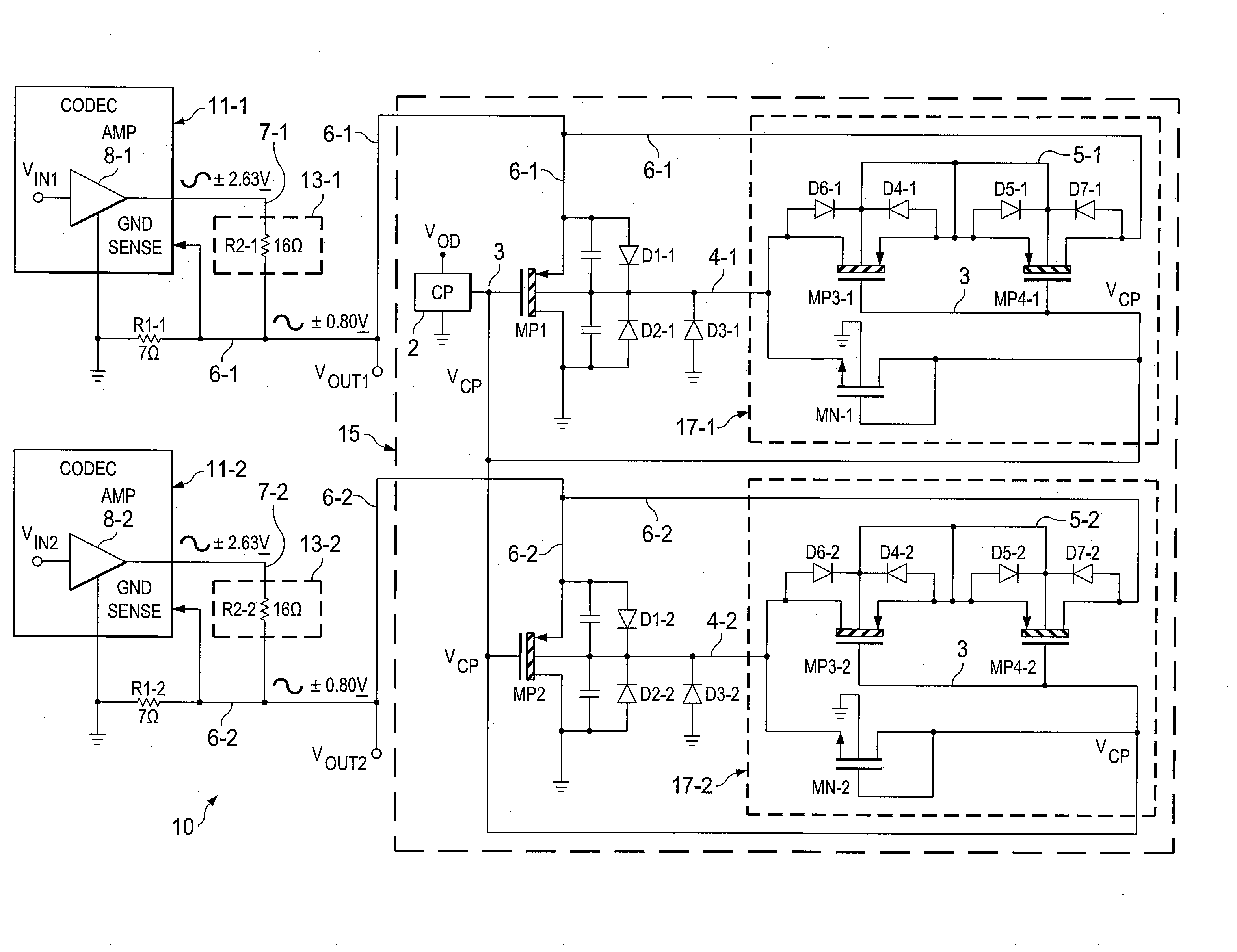
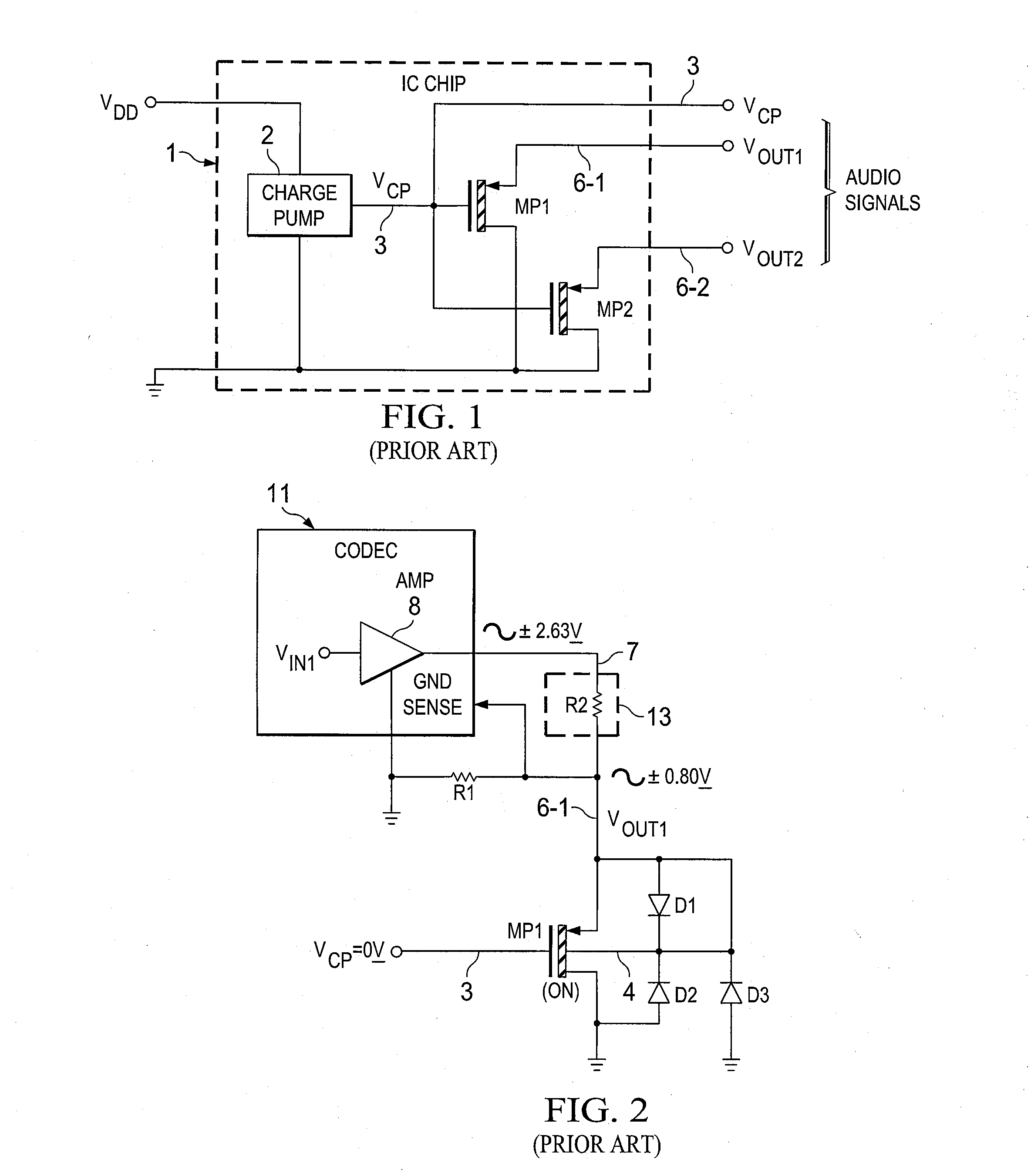
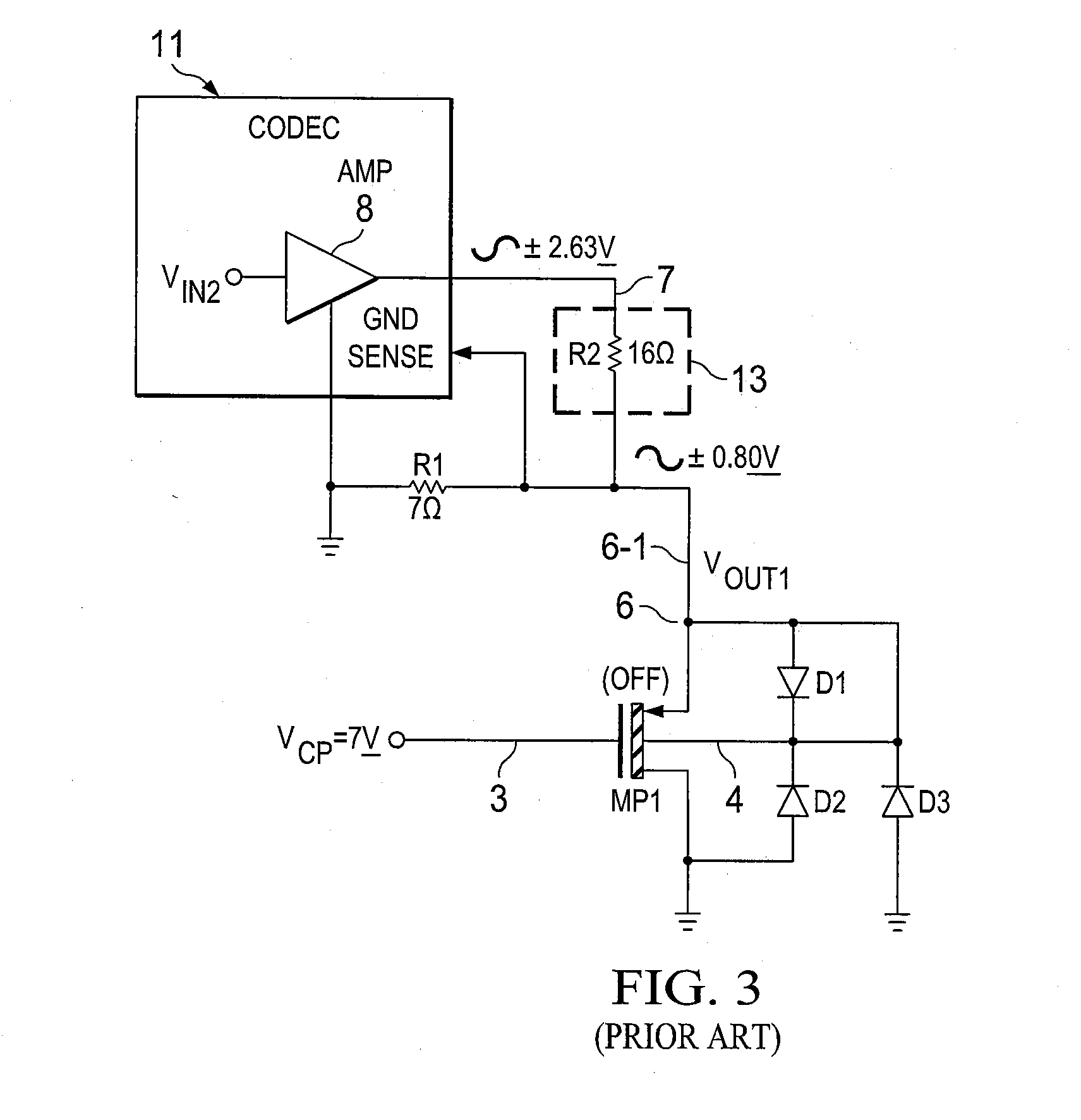
[0038]FIG. 4 shows an embodiment of a circuit 10 which includes ground switch circuitry 15 that in turn includes first and second audio signal channels and also includes negative voltage protection circuits 17-1 and 17-2. Negative voltage protection circuits 17-1 and 17-2 prevent negative portions of audio signals in the two channels from forward biasing internal parasitic PN junctions (i.e., PN diodes) in depletion mode “ground switch” transistors MP1 and MP2 of ground switch circuitry 15 and thereby prevent distortion of audio signals in the first and second audio signal channels caused by the negative portions of the audio signals.

[0039]The first audio signal channel includes an audio amplifier 8-1 producing an audio output signal on conductor 7-1, and also includes a resistive voltage divider including speaker resistance R2-1 coupled between output 7-1 of amplifier 8-1 and an output conductor 6-1 on which VOUT1 is produced. Audio amplifier 8-1 is included in a conventional CODEC...


PUM


Abstract

Self-grounded circuitry (10) includes a signal channel conducting an output voltage (VOUT1). A charge pump (2) powered by a reference voltage (VDD) produces a control voltage (VCP). The control signal is at a low level if the reference voltage is low and is boosted to a high level if the reference voltage is high. A ground switch circuit (15) includes a depletion mode transistor (MP1) having a source coupled to the output voltage, a gate coupled to the control voltage, and a drain coupled to ground. The transistor includes a well region (4-1) and a parasitic substrate diode (D3-1). A negative voltage protection circuit (17-1) includes a depletion mode first protection transistor (MP3-1) having a drain coupled to the well region, a source coupled to a source of a depletion mode second protection transistor (MP4-1) having a drain coupled to the output voltage, the first and second protection transistors each having a gate coupled to the control voltage, and also includes a diode (MN1) coupled to charge the well region from the control voltage conductor to prevent distortion of the output voltage.

Description

BACKGROUND OF THE INVENTION[0001]The present invention relates generally to “audio ground switches” that include depletion mode MOS transistors which function as audio ground switches connected to prevent build-up of charge that may result in discharging and associated popping sounds when a headset is plugged into an audio signal jack of a device generating the audio signal.[0002]The discharge of the above-mentioned charge build-up occurs because an audio ground switch, along with circuitry connected to it, have parasitic capacitances, inductances, and resistances that are subject to build up of static charge which can be discharged similarly to common electrostatic discharge (ESD). The above-mentioned built-up charge in audio ground switch circuitry may be electrostatically discharged to ground at the instant a headset is connected to circuitry connected to the audio ground switch. The resulting current through the headset speaker resistance may cause the above-mentioned clicking / p...

Claims


Application Information

Patent Timeline
Patent Type & Authority Applications(United States)
IPC IPC(8): H03F1/30H02H9/04
CPCH02H9/045H03F1/305H03K17/6874H03F2200/441H03F2200/444H03K2217/0018H03F1/523H03F3/187H03F3/68H03F2200/555
Inventor ELWART, II, DAVID H.VINAY, VIKAS SUMAGRAVES, CHRISTOPHER M.HAROUN, BAHER S.
Owner TEXAS INSTR INC
Why Eureka
Try Eureka