Mult-level recording in a superattice phase change memory cell
- Summary
- Abstract
- Description
- Claims
- Application Information
AI Technical Summary
Benefits of technology
Problems solved by technology
Method used
Image

Examples
first embodiment
Description of Prior Art Technique
[0031]In a “phase-change memory cell” using a phase-change material as a recording material, data is recorded by utilizing Joule heat generated by applying a voltage pulse to the recording material to cause an electric current to flow through the recording material.
[0032]In the case where the recording material is in a crystalline state, by melting the recording material by Joule heat and then quickly cooling the recording material, an amorphous state is produced. Moreover, in the case where the recording material is in an amorphous state, by applying a voltage pulse equal to or higher than a threshold voltage inherent to the recording material to utilize Joule heat generated by an electric current that is caused to flow through the recording material and gradually cooling the recording material by controlling the conditions of the voltage pulse, a crystalline state is produced.
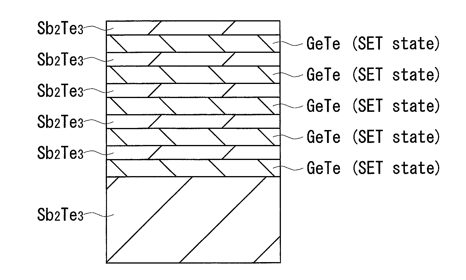
[0033]GeSbTe (germanium-antimony-tellurium) is mainly used as the phase-...
second embodiment
[0076]In the second embodiment, the verify is carried out to the superlattice phase-change memory cell described in the aforementioned first embodiment.
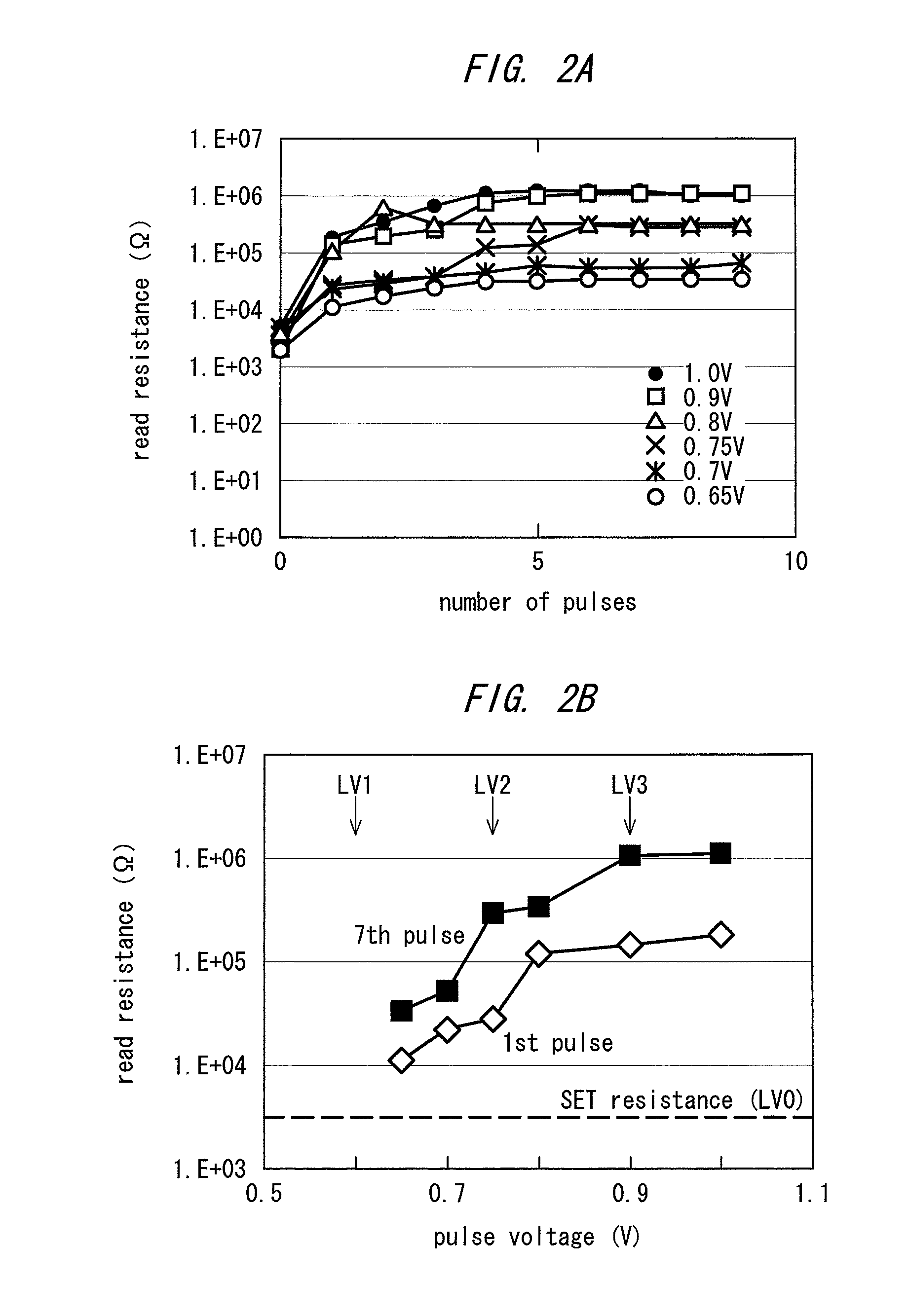
[0077]First, the number of pulse times of recording pulses required for a multi-level record will be described.
[0078]The number of pulse times of the recording pulses is dependent on the design of the superlattice phase-change memory cell and the stacked structure of the superlattice phase-change material. Therefore, the nominal number of pulse times is preliminarily recorded in a buffer memory in the phase-change device, and after applying the recording pulses until reaching the nominal number of pulse times, the verify is carried out, and the recording is continued until a desired read resistance is obtained.
[0079]Alternatively, it is also possible to learn the nominal number of pulse times. Prior to the shipment of the phase-change device or during a period in which data input and output are not executed so frequently in the use o...
third embodiment
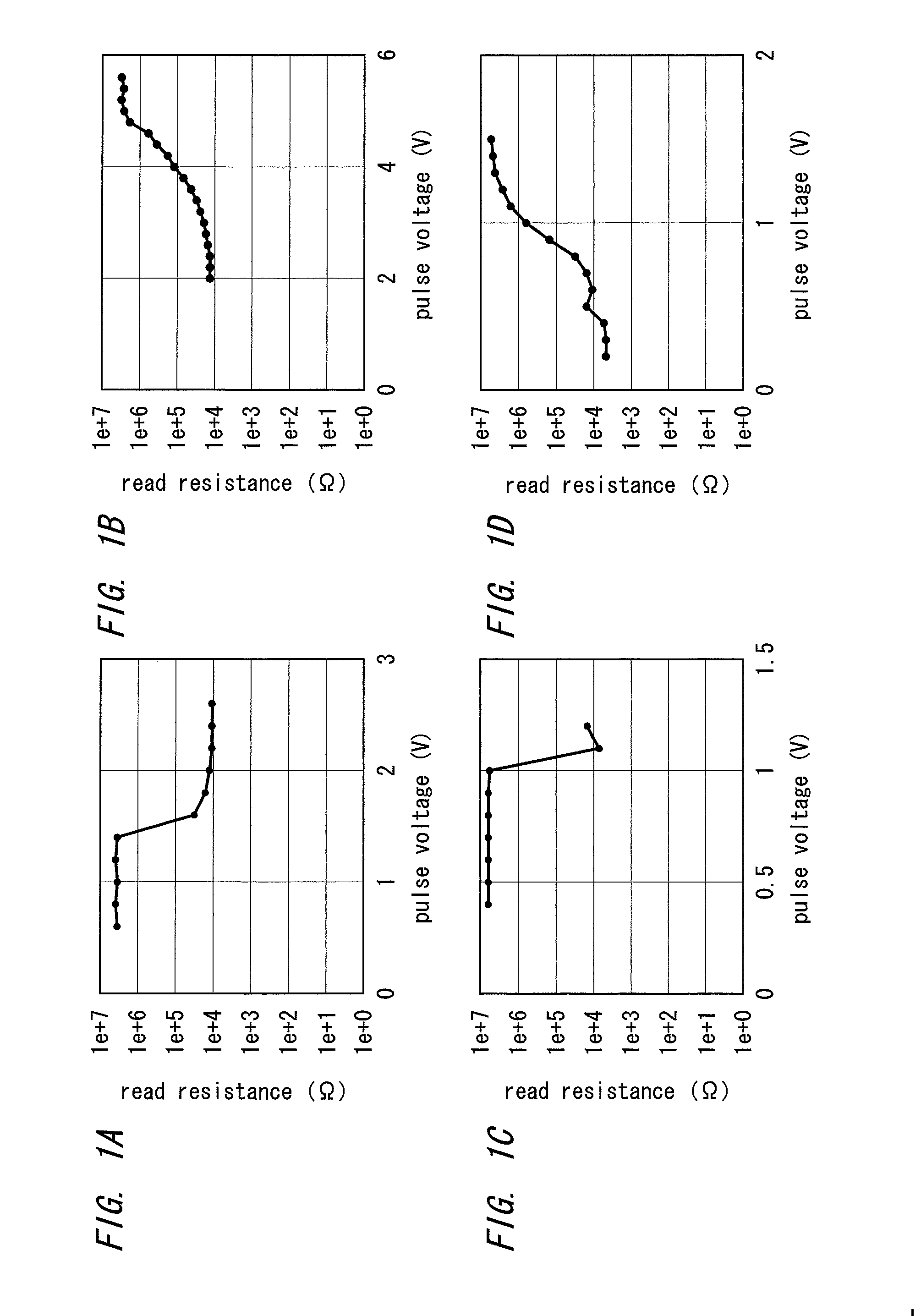
[0090]In the third embodiment, the method of verify different from the method of verify described in the aforementioned second embodiment will be described. FIG. 7 is a drawing showing an algorithm in the case of carrying out the verify in the third embodiment. In the following description, a nominal read resistance is referred to as “nominal resistance”, a voltage value of a recording pulse required for recording a certain nominal resistance in a superlattice phase-change memory cell is referred to as “nominal voltage”, and the nominal number of times of pulses is referred to as “the nominal number of pulse times”.
[0091]First, the nominal voltage Vpulse is set to V0 and the nominal number of pulse times Npulse is set to Npulse0. Next, the recording pulse of the nominal voltage Vpulse is applied the nominal number of pulse times Npulse, and a read resistance Rread thus formed is measured. Here, in the case where the read resistance Rread is within the range of the desired nominal re...
PUM
 Abstract
Description
Claims
Application Information
 - R&D Engineer
- R&D Manager
- IP Professional
- Industry Leading Data Capabilities
- Powerful AI technology
- Patent DNA Extraction
Browse by: Latest US Patents, China's latest patents, Technical Efficacy Thesaurus, Application Domain, Technology Topic.
© 2024 PatSnap. All rights reserved.Legal|Privacy policy|Modern Slavery Act Transparency Statement|Sitemap