Novel NAND array architecture for multiple simutaneous program and read

a nand array and program and read technology, applied in the field of all 2d and 3d nand array architecture circuits, can solve the problems of multiple high bl precharge currents, multiple blocks in different nand planes in different rows cannot be selected, and the nand array and sensing latch circuits do not offer all-bl reads, etc., to achieve the effect of increasing the speed of precharge and discharge, reducing the size of the on-chip pb

Active Publication Date: 2015-01-01
APLUS FLASH TECH
View PDF1 Cites 48 Cited by
  • Summary
  • Abstract
  • Description
  • Claims
  • Application Information

AI Technical Summary

Benefits of technology

[0053]In another specific embodiment, the present invention provides a technique for single LV GBL-PB to store K-page temporary data for M-WL & All-BL Program and Program-Verify operations. The K-page is preferably to have more than one page but the value of K<M for an optimal PB size. Additional pages of PB are used to temporarily store the K pages of read or program-verified page data and then be serially or parallelly loaded into I/O bus and read in pipeline form by off-chip Flash controller. As a result, the on-chip PB size can be reduced for this preferred Multiple-WL & All-BL Program, Program-Verify, and Read operations.
[0054]In yet another specific embodiment, the present in

Problems solved by technology

Nevertheless, unless each Plane has its own PB circuit, multiple Blocks in different NAND Planes in different rows cannot be selected because PB and BLs are shared by all NAND Blocks cascaded vertically in the Y-direction.
Therefore this conventional NAND array and sensing Latch circuit do not offer ALL-BL Read.
The disadvantage Program-Inhibit BL=Vdd lies in that multiple high BL precharged currents are required because it needs to change the selected BL to Vdd.d) NAND Program scheme: A low current FN channel tunneling effect to increase NAND cell's Vt from E state (erased state) to three program states such as A, B, or C state for a MLC storage.e) Program-Inhibit voltage generation methods

Method used


Image

  • Novel NAND array architecture for multiple simutaneous program and read
  • Novel NAND array architecture for multiple simutaneous program and read
  • Novel NAND array architecture for multiple simutaneous program and read

Examples


Embodiment Construction

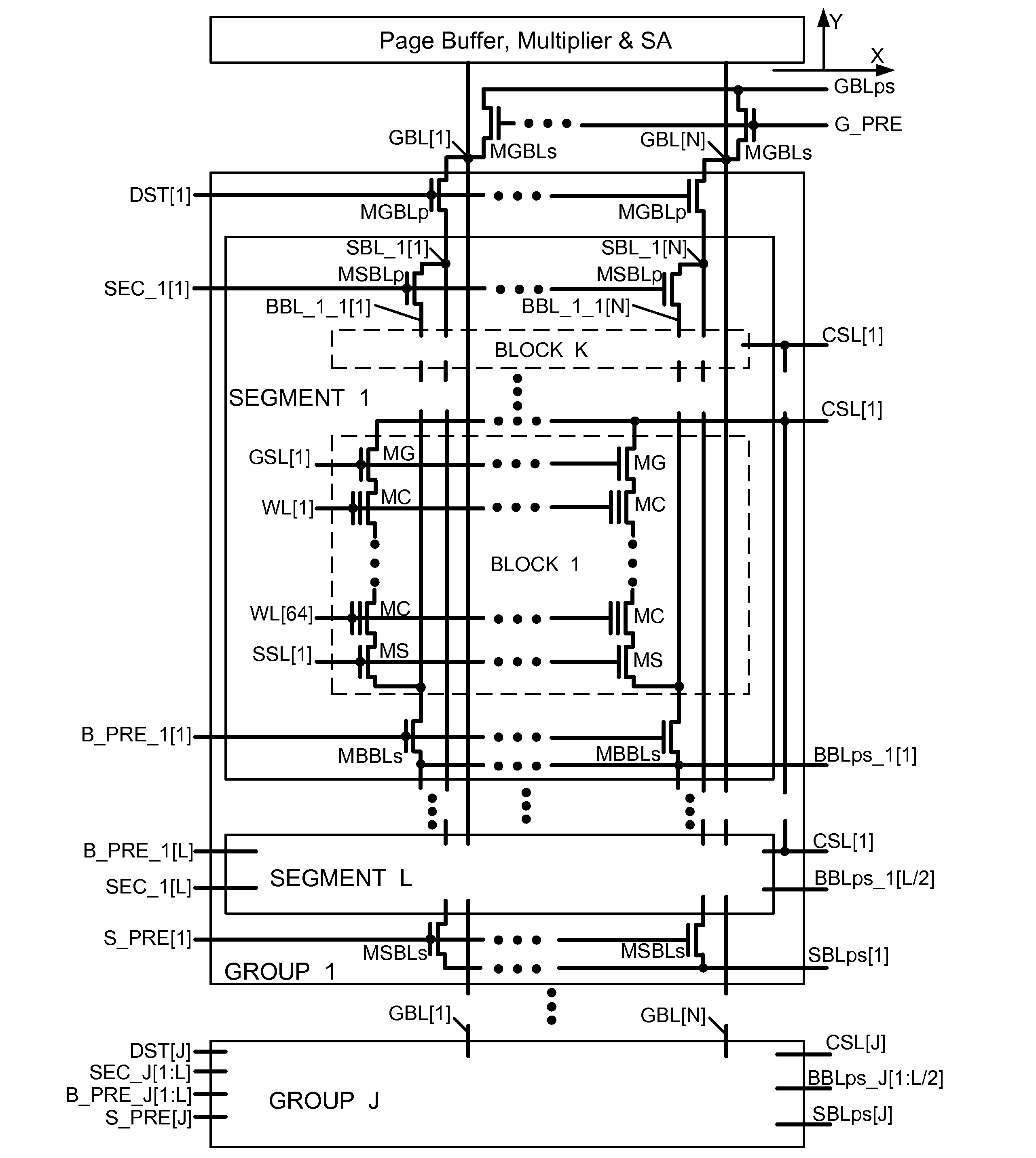
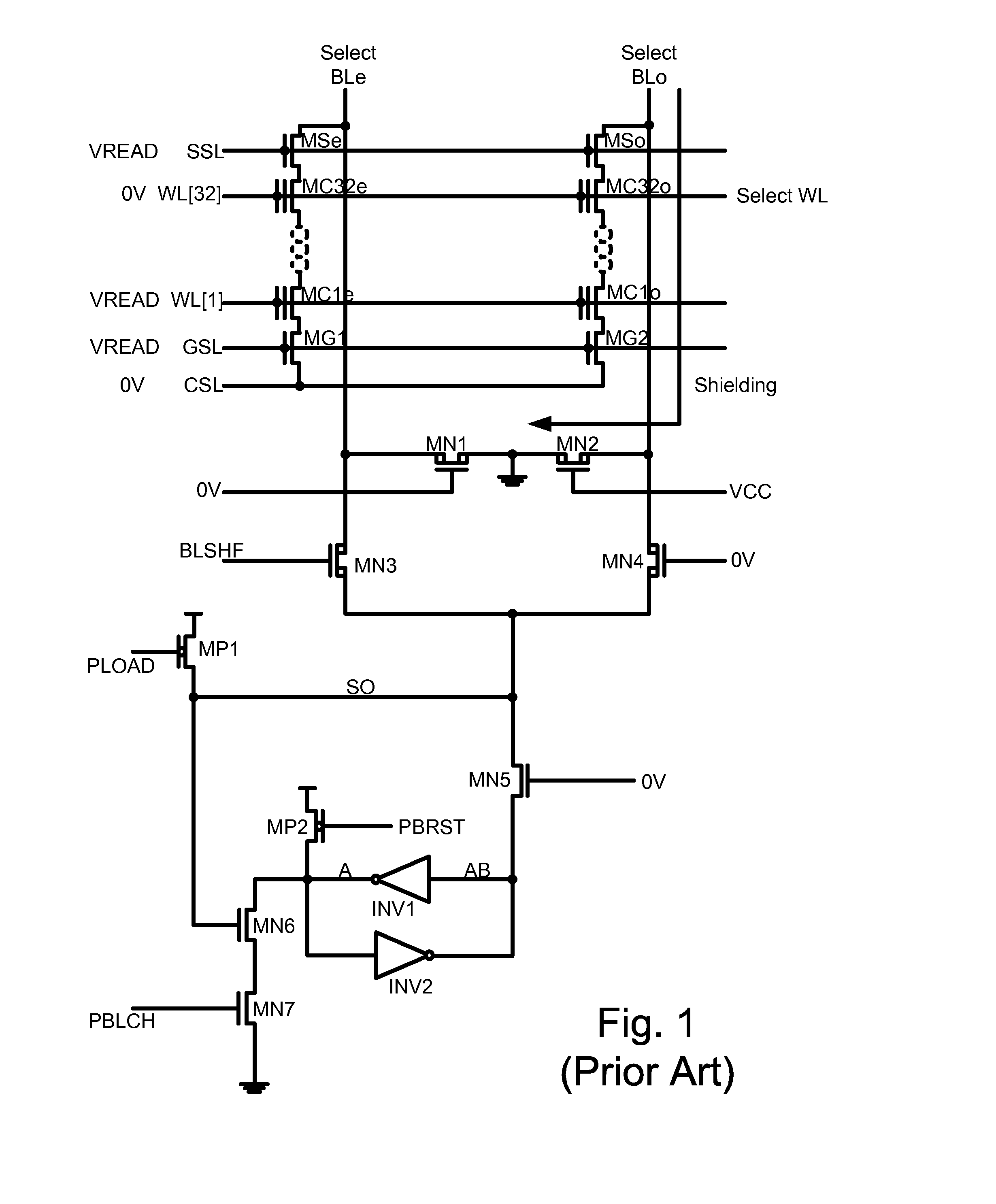
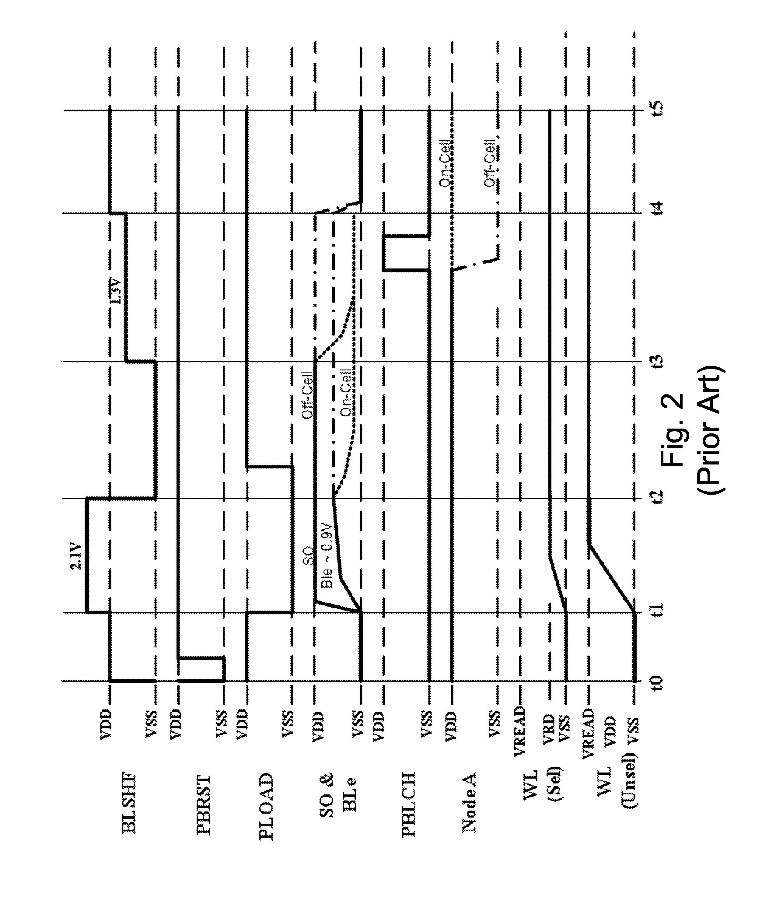
[0083]In the following detailed description, numerous specific details are set forth in order to provide a more thorough understanding of the present invention. The detailed description of the present invention, reference is made towards the accompanying drawings, flows and tables that form a part hereof and in which is shown, by way of illustration, specific embodiments in which the invention may be practiced. In the drawings, like numbers describe substantially similar components throughout the several views and embodiments. These embodiments are described in sufficient detail with a goal to enable those skilled in the art to practice the invention. Other embodiments may be made without departing from the scope of the present invention. The following detailed description is not to be taken in a limiting sense, and the scope of the present invention is defined only by the appended claims and equivalents thereof. In other instances, well-known structures and devices are shown in blo...


PUM


Abstract

This invention discloses a HiNAND array scheme with multiple-level of bit lines (BLs) including metal3 global bit lines (GBLs), divided metal2 Segment bit lines (SBLs), and divided metal1 block bit lines (BBLs) laid out in parallel to each other respectively for a plurality of NAND Strings. All other source lines or power lines connected to bottoms of corresponding String capacitances of GBLs, SBLs, and BBLs are associated with metal0 line laid out perpendicular to those BLs. Under the HiNAND array scheme, conventional one-WL Read and Program-Verify operations are replaced by multiple-WL and All-BL Read and Program-Verify operations executed with charge capacitance of SBLs being reduced to 1/10- 1/20 of capacitance of GBLs to achieve DRAM-like faster operation, less operation stress, and lower power consumption. A preferred set of program biased voltages on the selected WL and remaining non-selected WLs associated with a Multiplier and a DRAM-like charge-sharing Latch Sensing Amplifier is proposed.

Description

1. CROSS-REFERENCES TO RELATED APPLICATIONS[0001]This application claims priority to U.S. Provisional Application No. 61 / 840,020, filed Jun. 27, 2013, commonly assigned and incorporated by reference herein for all purposes.[0002]Additionally, this application is related to U.S. Pat. Nos. 7,440,318, 7,570,517, RE43,665 E, and 7,262,994, which are incorporated by reference herein for all purposes.[0003]This application is further related to an article titled “A 3.3V 128 Mb Multi-Level NAND Flash Memory for Mass Storage Applications” by Tae-Sung Jung, etc., Samsung Electronics, Solid-State Circuits Conference, Feb. 10, 1996. Digest of Technical Papers. 42nd ISSCC. 1996 IEEE International, page 32-33; and an article titled “A 1.8V 2 Gb NAND Flash Memory for Mass Storage Applications” by June Lee et al., IEEE J Solid-State Circuits, vol. 38, No. 11, November 2003, pp. 1934-1942.2. BACKGROUND OF THE INVENTION[0004]This invention relates generally to all 2D and 3D NAND array architecture c...

Claims


Application Information

Patent Timeline
IPC IPC(8): G11C16/26G11C16/10
CPCG11C16/26G11C16/10G11C8/12G11C11/5628G11C16/0483G11C16/3459G11C11/5642G11C16/24G11C16/3445
Inventor LEE, PETER, WUNG
Owner APLUS FLASH TECH
Why Eureka
Try Eureka