Semiconductor device with vertical gate and method of manufacturing the same

a technology of semiconductor devices and gate electrodes, which is applied in the direction of semiconductor devices, electrical devices, transistors, etc., can solve the problems of limited gate electrode pitch decrease and void formation in source electrodes, and achieve the effect of reducing gate electrode resistance, and reducing gate electrode pitch

Active Publication Date: 2015-01-08
PANASONIC SEMICON SOLUTIONS CO LTD
View PDF1 Cites 6 Cited by
  • Summary
  • Abstract
  • Description
  • Claims
  • Application Information

AI Technical Summary

Benefits of technology

[0012]By employing the method of manufacturing a semiconductor device with vertical gate according to this aspect, it is possible to form the source region without using a lithography technique. Accordingly, it is not necessary to secure a margin of mask superposition shift and it is possible to further reduce the gate electrode pitch, compared with the conventional technique. As a result, it is possible to implement a semiconductor device with vertical gate with smaller on-resistance. The first source region may be formed in a self-alignment manner by introduction of impurities through the etched-back first insulating film, instead of the introduction of impurities through the non-etched-back first insulating film.
[0015]By employing the semiconductor device with vertical gate according to this aspect, it is possible to form the source region without using a lithography technique. Accordingly, it is not necessary to secure a margin of mask superposition shift and it is possible to further reduce the gate electrode pitch, compared with the conventional technique. As a result, it is possible to implement a semiconductor device with vertical gate with smaller on-resistance. In the semiconductor device with vertical gate, the interface between the source region and the first body region may be formed in a planar shape inclined with respect to the side wall of the trench.
[0016]According to the aspects of the present invention, since the first and second source regions as the source region can be formed in a self-alignment manner without using a lithography technique, it is possible to further reduce the gate electrode pitch, compared with the conventional technique. As a result, it is possible to implement a semiconductor device with vertical gate with smaller on-resistance at a low cost.

Problems solved by technology

These concave portions cause a problem in that voids are formed in the source electrodes embedded in the concave portions, or the like.
However, in the semiconductor device with vertical gate disclosed in Unexamined Japanese Patent Publication No. 2005-209807, Unexamined Japanese Patent Publication No. 2007-500454 and Japanese Patent No. 4,545,679, when the gap between the neighboring gate electrodes needs to be further reduced with requirements for a decrease in size, it is necessary to secure a margin of mask superposition shift for used masks and thus the decrease in gate electrode pitch is limited.

Method used


Image

  • Semiconductor device with vertical gate and method of manufacturing the same
  • Semiconductor device with vertical gate and method of manufacturing the same
  • Semiconductor device with vertical gate and method of manufacturing the same

Examples


Embodiment Construction

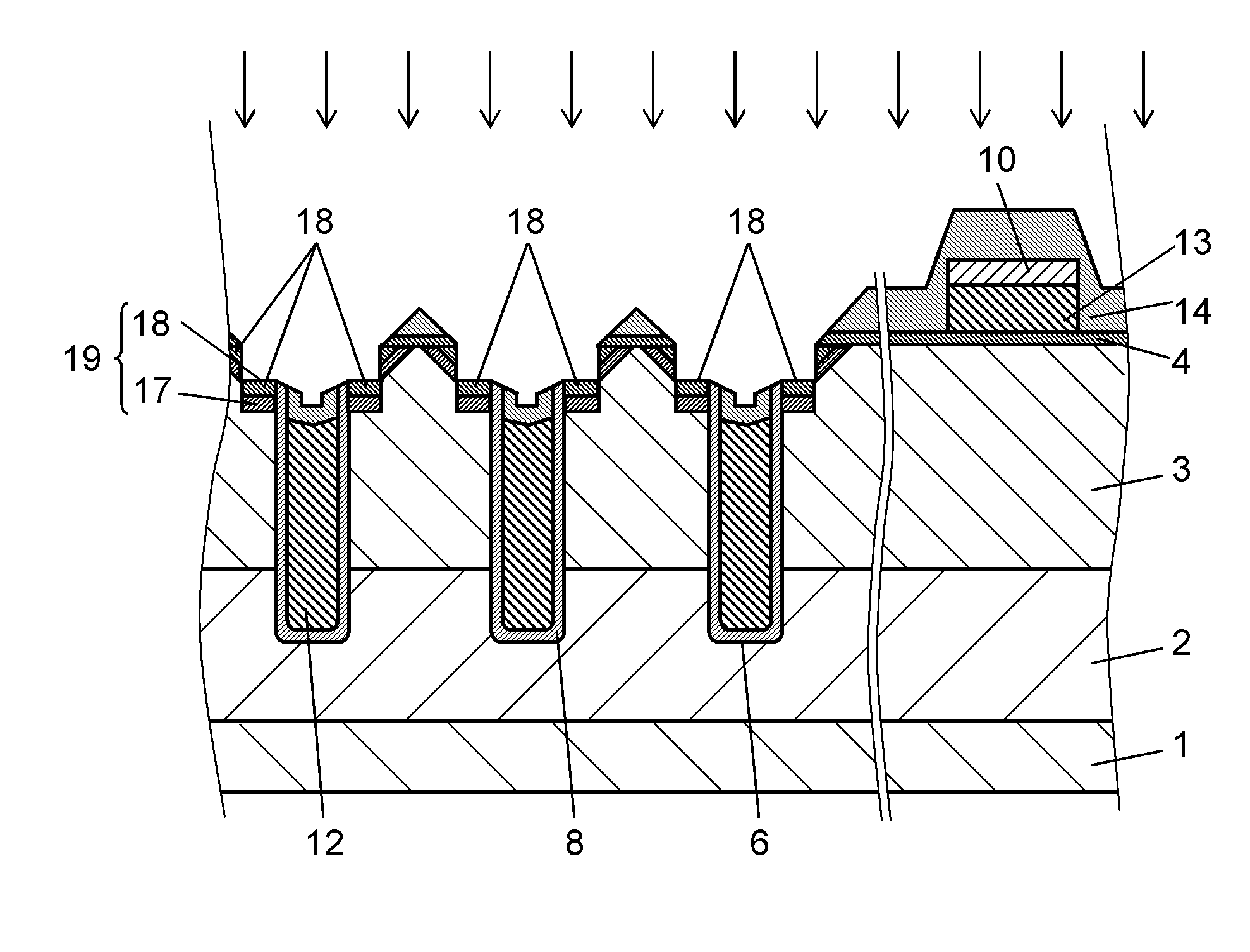
[0075]Hereinafter, a semiconductor device according to an exemplary embodiment of the present invention along with a method of manufacturing the semiconductor device will be described with reference to the accompanying drawings. In the following exemplary embodiment, the present invention is embodied by an N-channel vertical-gate transistor. In this example, a first conductivity type mentioned in the present invention is an N type and a second conductivity type is a P type. The following description can be similarly applied to a P-channel vertical-gate transistor by inverting the conductivity types of impurity regions in the elements.

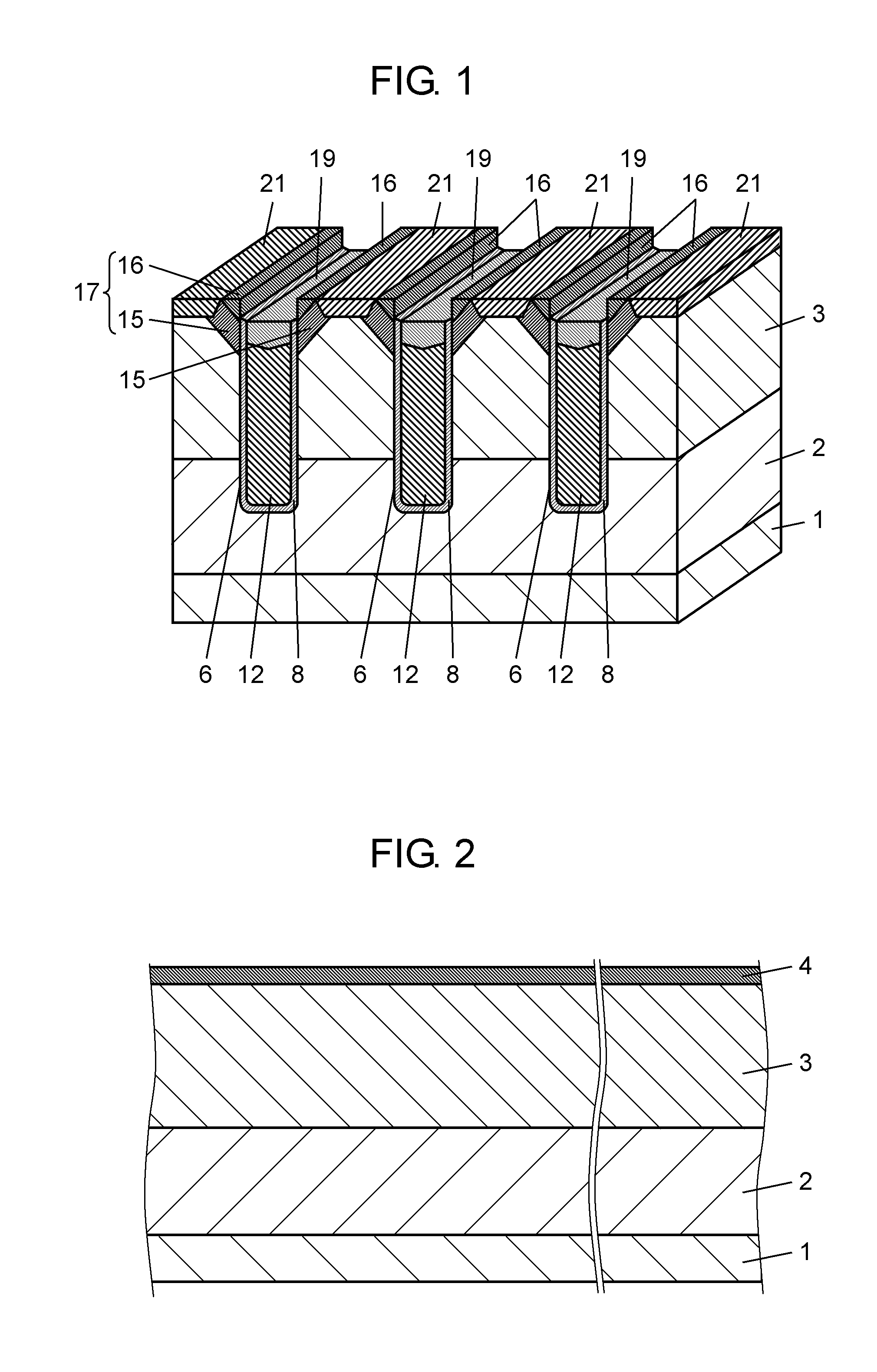
[0076]FIG. 1 is a diagram schematically illustrating the configuration of a semiconductor device according to an exemplary embodiment of the present invention. In FIG. 1, a source electrode and a structure thereon are not shown. FIG. 1 is a schematic diagram and the dimensional ratio of constituents is not limited to one shown in the drawing.

[0077]As sh...


PUM

PropertyMeasurementUnit
depthaaaaaaaaaa
widthaaaaaaaaaa
thicknessaaaaaaaaaa

Abstract

A gate electrode is formed in a trench reaching a drain region so as to leave a concave portion on the top of the trench. A first insulating film is formed, which fills the concave portion and of which the thickness increases as the distance from an end of the trench increases on the substrate surface on both sides of the trench. First and second source regions are formed in a self-alignment manner by introduction of impurities through the first insulating film.

Description

[0001]This application is a U.S. national phase application of PCT international application PCT / JP2012 / 002382 filed on Apr. 5, 2012, which claims priority to Japanese Patent Application No. 2011-094415 filed on Apr. 20, 2011. The disclosures of these applications including the specifications, the drawings, and the claims are hereby incorporated by reference in its entirety.BACKGROUND[0002]1. Technical Field[0003]The present invention relates to a semiconductor device with vertical gate having a vertical gate electrode and a method of manufacturing the semiconductor device with vertical gate.[0004]2. Description of the Related Art[0005]With recent requirements for a decrease in power consumption, an improvement in functional performance, and an increase in operation speed in electronic apparatuses, a decrease in power consumption and an increase in operation speed have been also required in semiconductor devices built therein. In order to cope with these requirements, it is necessar...

Claims


Application Information

Patent Timeline
Patent Type & Authority Applications(United States)
IPC IPC(8): H01L29/66H01L29/10H01L21/266H01L21/28H01L21/321H01L21/3213H01L29/423H01L21/265
CPCH01L29/66666H01L29/4236H01L29/1095H01L21/266H01L21/28035H01L21/3212H01L21/32133H01L21/2652H01L29/0865H01L29/0869H01L29/66734H01L29/7813H01L29/086
Inventor MIZOKUCHI, SHUJIOOKAWA, RYOUSUKESATO, NAOKI
Owner PANASONIC SEMICON SOLUTIONS CO LTD
Why Eureka
Try Eureka