
Ceramic electronic component and method for manufacturing the same

Active Publication Date: 2015-01-15
MURATA MFG CO LTD
View PDF14 Cites 32 Cited by
  • Summary
  • Abstract
  • Description
  • Claims
  • Application Information

AI Technical Summary

Benefits of technology

The ceramic electronic component described in this patent has a layer of metal at the interface between the external and internal electrodes. This increases the bonded area and reduces the connection resistance between the electrodes, leading to a significant reduction in overall ESR (equivalent series resistance) of the component.

Problems solved by technology

As a result, the equivalent series resistance (ESR) of the main body of the laminated-type capacitor increases, which is problematic.
If such a reaction layer is formed at the interface between the ceramic main body and the external electrodes, the bonded area between the internal electrodes and the external electrodes may be hindered by the glass in the reaction layer, making the above-described problem of an increased ESR more noticeable.
However, since the laminated-type capacitor with the small height dimension H can easily develop a crack or a chip, it cannot be sufficiently subjected to the treatment for exposing the internal electrodes.
It is thus difficult to provide a sufficient bonded area between the internal electrodes and the external electrodes in the laminated-type capacitor with the small height dimension H.

Method used


Image

  • Ceramic electronic component and method for manufacturing the same
  • Ceramic electronic component and method for manufacturing the same
  • Ceramic electronic component and method for manufacturing the same

Examples


Embodiment Construction

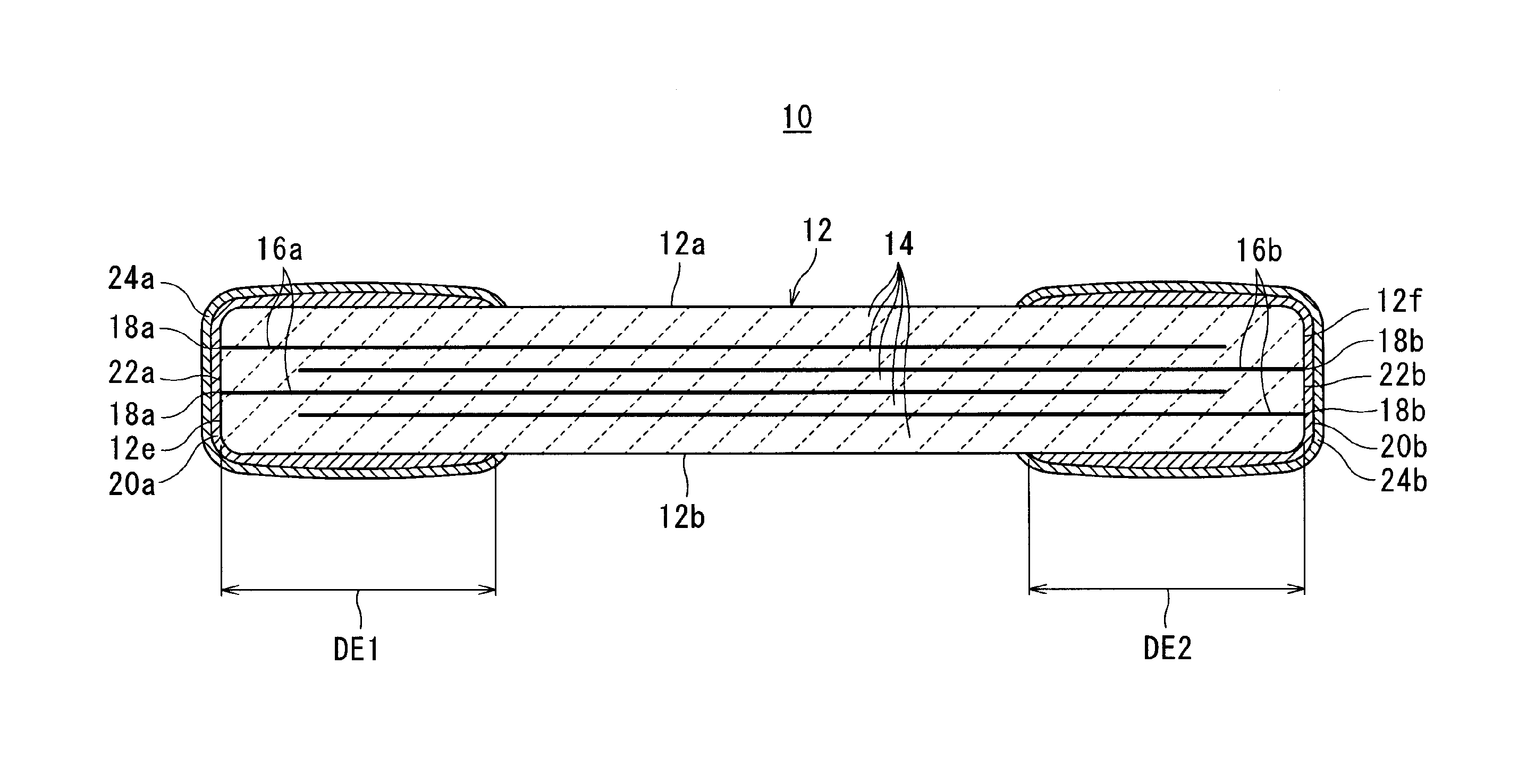
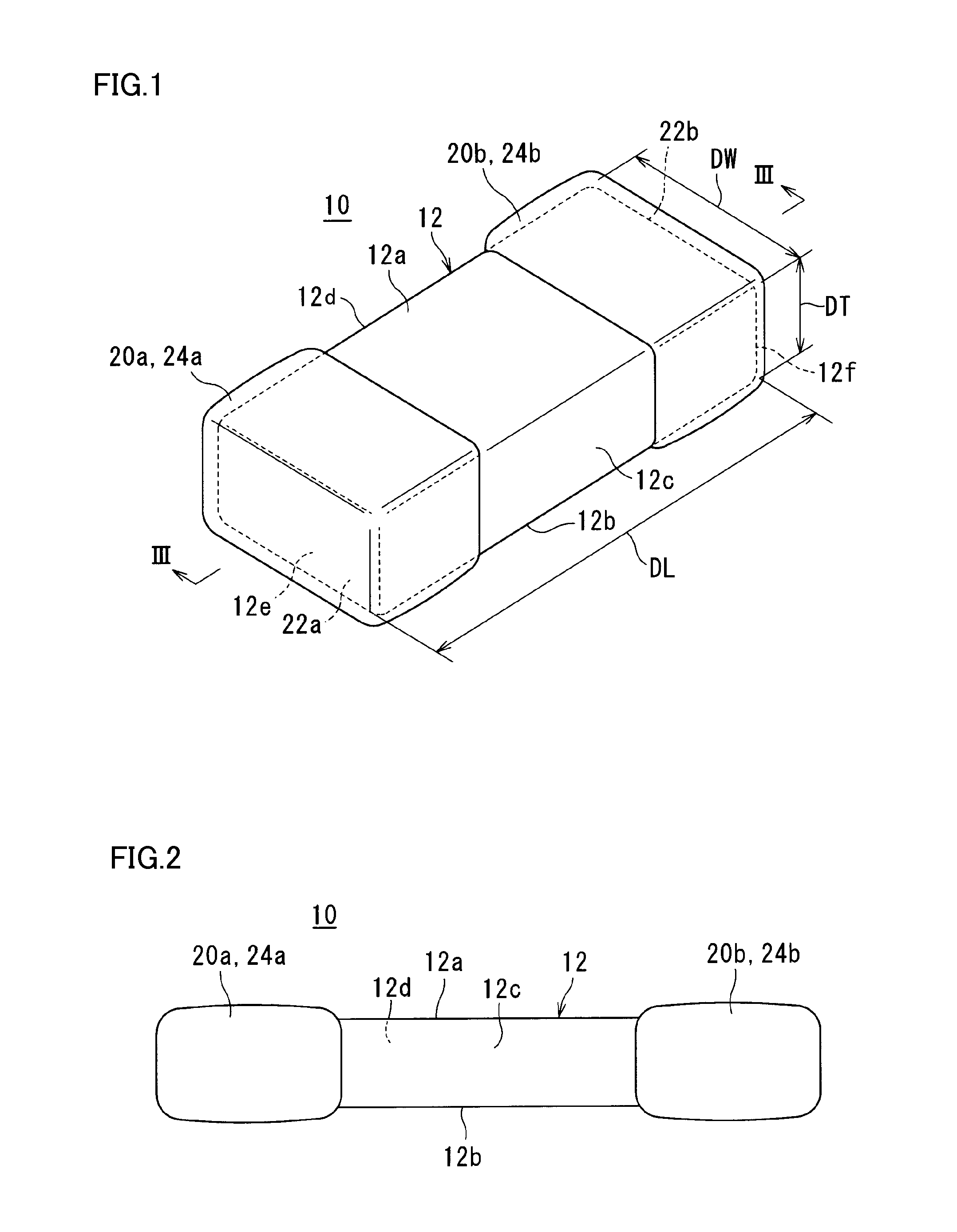
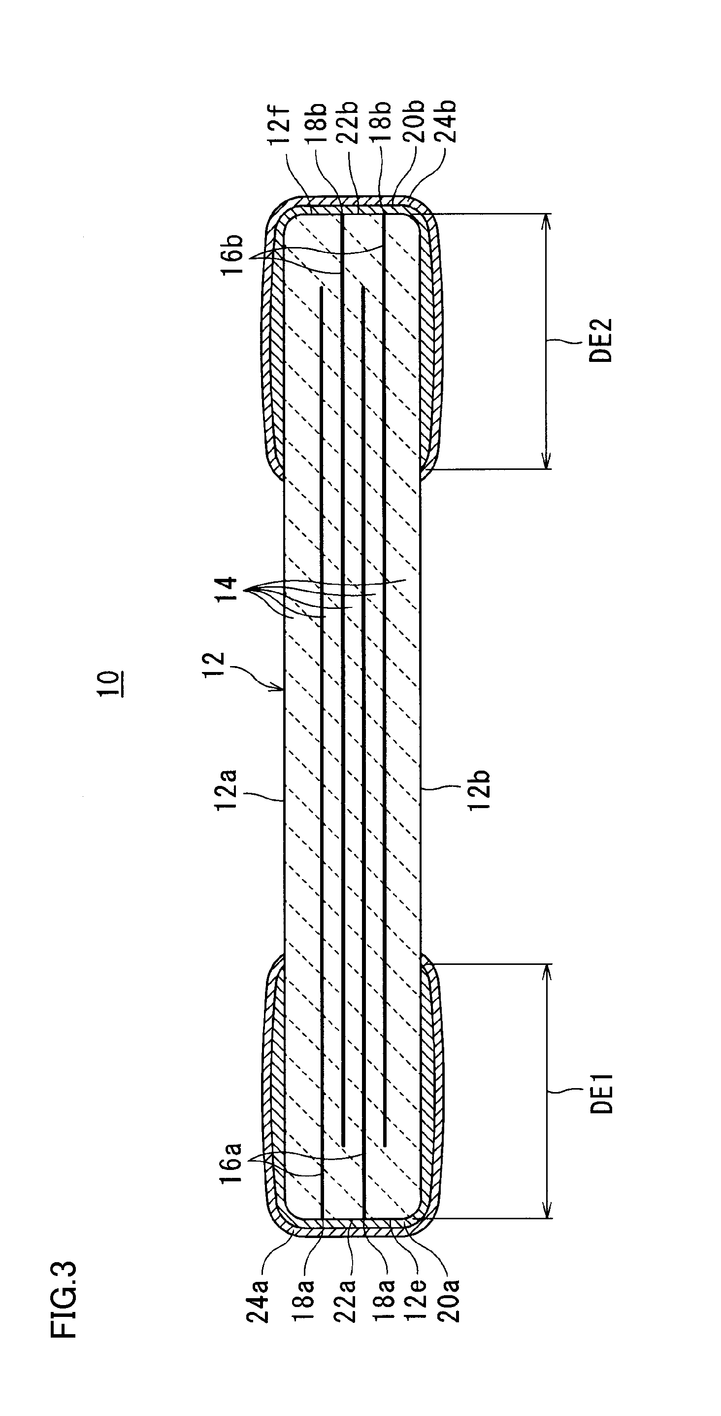
[0025]A laminated ceramic capacitor 10 shown in FIG. 1 includes a thin ceramic main body 12 having a rectangular or substantially rectangular parallel or substantially parallelepiped shape, for example. Ceramic main body 12 preferably includes a plurality of laminated ceramic layers 14, and includes a pair of main surfaces 12a, 12b opposed to each other, a pair of side surfaces 12c, 12d opposed to each other, and a pair of end surfaces 12e, 12f opposed to each other.

[0026]While ceramic main body 12 preferably is configured with the rectangular or substantially rectangular parallel or substantially parallelepiped shape in laminated ceramic capacitor 10 in this preferred embodiment, the shape of ceramic main body 12 is not particularly limited thereto.

[0027]Moreover, ceramic main body 12 preferably has rounded corner portions and rounded ridge portions.

[0028]In ceramic main body 12, a length in a direction in which the pair of main surfaces 12a, 12b of ceramic main body 12 are connect...


PUM

PropertyMeasurementUnit
Lengthaaaaaaaaaa
Lengthaaaaaaaaaa
Fractionaaaaaaaaaa

Abstract

External electrodes, electrically connected to exposed portions of internal electrodes, are arranged on end surfaces of a ceramic main body of a laminated ceramic capacitor. Alloy layers of a metal contained in internal electrodes, and a metal contained in external electrodes, are arranged at the boundaries between external electrodes, and the ceramic main body and internal electrodes. Plating layers are provided on surfaces of external electrodes. A ceramic electronic component having a reduced ESR is thus provided.

Description

BACKGROUND OF THE INVENTION[0001]1. Field of the Invention[0002]The present invention relates to a ceramic electronic component and a method for manufacturing the ceramic electronic component, and particularly to a ceramic electronic component such as a laminated ceramic capacitor or a laminated ceramic inductor, for example, and a method for manufacturing such a ceramic electronic component.[0003]2. Description of the Related Art[0004]In recent years, as electronic devices such as portable telephones, portable music players, and the like have decreased in size and thickness, ceramic electronic components mounted on such electronic devices also rapidly continue to decrease in size and thickness. Japanese Patent Laying-Open No. 2012-222276, for example, discloses a laminated-type capacitor whose length dimension L is 1.0 mm, width dimension W is 5.0 mm, and thickness dimension T (height dimension H) is 0.15 mm. Furthermore, Japanese Patent Laying-Open No. 2000-40635 discloses a ceram...

Claims


Application Information

Patent Timeline
IPC IPC(8): H01G4/005H01L41/047H01C7/00H01G4/30H01F27/29
CPCH01L41/0472H01G4/005H01F27/29H01G4/30H01C7/008H10N30/872H10N30/063H01F27/2804H01F2027/2809H01G4/008H01G4/12H01G4/248
Inventor ONISHI, KOSUKESASAKI, TOMOHIRONISHISAKA, YASUHIROISHIZUKA, AKIRAYOSHIDA, AKIHIRO
Owner MURATA MFG CO LTD
Learn More