Method for fabricating thin-film transistor

a thin-film transistor and fabrication method technology, applied in the direction of semiconductor devices, electrical appliances, basic electric elements, etc., can solve the problems of reducing the insulation affecting the performance of the film, so as to reduce the density of the film, prevent the effect of deterioration of the film properties, and reduce the effect of film density

Active Publication Date: 2015-01-15
NISSIN ELECTRIC CO LTD
View PDF2 Cites 9 Cited by
  • Summary
  • Abstract
  • Description
  • Claims
  • Application Information

AI Technical Summary

Benefits of technology

[0047]According to the eleventh item of the invention, similar to the above fourth item of the invention, the following effects may be further achieved. The dangling bond in the film may be moderately buried by the fluorine, and since the fluorine is not excessive, deterioration of film properties, such as reduction in film density and reduction in insulation performance, may be prevented.
[0048]In order to make the aforementioned and other objects, features and advantages of this invention comprehensible, a preferred embodiment accompanied with figures is described in detail below.

Problems solved by technology

However, a problem is known that when such hydrogenated SiN film is used as the diffusion prevention film in the method for fabricating a TFT by the aforementioned self-alignment process, the excimer laser light cannot be transmitted through the diffusion prevention film and is almost absorbed by the film.
Consequently, not only the source / drain regions cannot be formed, but also problems such as damage to the diffusion prevention film, peeling-off of the film from the substrate, and even breakdown of transistor devices, etc. are caused due to an excessive temperature rise in the diffusion prevention film.

Method used


Image

  • Method for fabricating thin-film transistor
  • Method for fabricating thin-film transistor
  • Method for fabricating thin-film transistor

Examples


first embodiment

(1) First Embodiment

Bottom Gate Structure 1

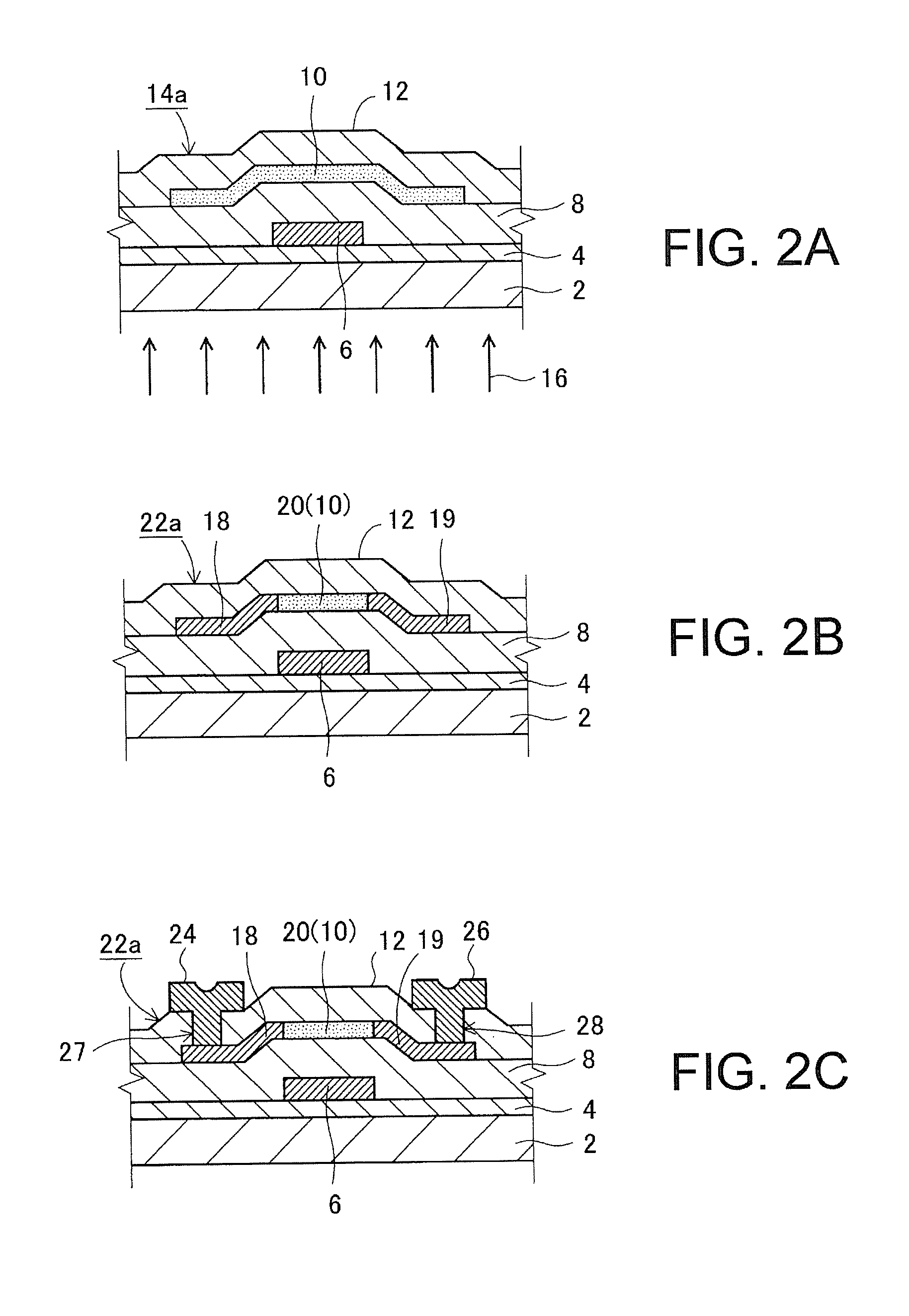
[0057]The first embodiment is directed to an example of a method for fabricating a TFT having a bottom gate structure, and is described with reference to FIGS. 2A to 2C and FIGS. 3A and 3B.

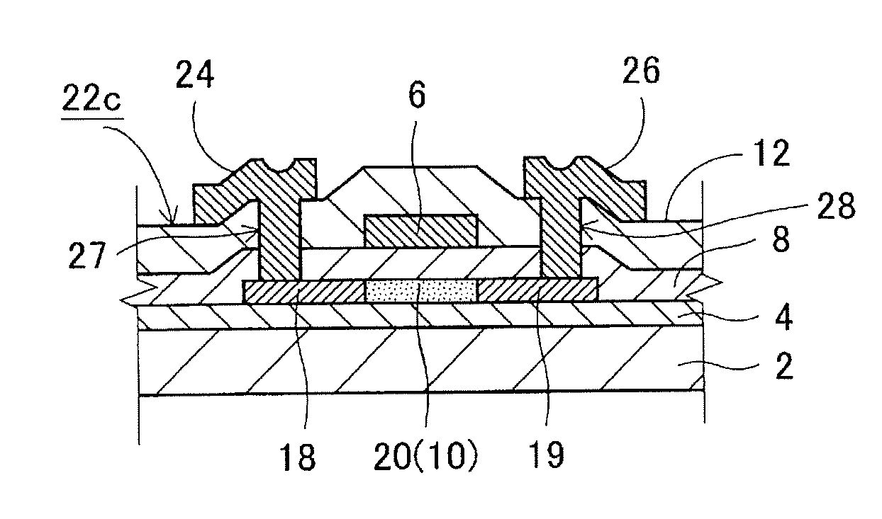
[0058]A structure 14a is provided, including a substrate 2 transmitting an excimer laser light 16, a diffusion prevention film 4 formed on the substrate 2 to prevent diffusion of impurities from the substrate 2 (i.e., substances contained in the substrate 2, e.g., alkali metal such as sodium, etc.), a gate electrode 6 with a predetermined pattern and a gate insulating film 8 covering the gate electrode 6 that are formed on the diffusion prevention film 4, and an oxide semiconductor layer 10 with a predetermined pattern formed on the gate insulating film 8 (see FIG. 2(A)).

[0059]Moreover, in this embodiment, although it is preferred that the structure 14a before being irradiated with the excimer laser light 16 further has a protection film 12 covering the o...

second embodiment

(3) Second Embodiment

Bottom Gate Structure 2

[0099]The second embodiment is directed to another example of the method for forming a TFT having a bottom gate structure, and is described referring to FIG. 5A to 5C.

[0100]In this embodiment, the structure 14b does not have the above diffusion prevention film 4, and is provided including a substrate 2 transmitting the excimer laser light 16, a gate electrode 6 having a predetermined pattern and a gate insulating film 8 covering the gate electrode 6 formed on the substrate 2, and an oxide semiconductor layer 10 having a predetermined pattern formed on the gate insulating film 8 (FIG. 5A).

[0101]In this embodiment, the gate insulating film 8 includes a SiN:F film containing fluorine in a SiN film as described above.

[0102]Whether or not the protection film 12 is formed in the structure 14b before the irradiation with the excimer laser light 16 is as mentioned above.

[0103]Also, in this embodiment, the structure 14b is irradiated with the excim...

third embodiment

(4) Third Embodiment

Top Gate Structure

[0108]The third embodiment is directed to an example of a method for fabricating a TFT having a top gate structure, and is described with reference to FIGS. 6A to 6C.

[0109]In this embodiment, the structure 14c is provided including a substrate 2, an oxide semiconductor layer 10 with a predetermined pattern formed on the substrate 2, a gate insulating film 8 formed on the oxide semiconductor layer 10, and a gate electrode 6 having a predetermined pattern formed on the gate insulating film 8 (FIG. 6A).

[0110]In this embodiment, the gate insulating film 8 includes a SiN:F film containing fluorine in a SiN film as described above.

[0111]Moreover, in this embodiment, since the irradiation by excimer laser light 16 is from the side of the gate electrode 6 instead of the substrate 2, in the self-alignment process, the substrate 2 does not necessarily transmit the excimer laser light 16.

[0112]In addition, as in this embodiment, the structure 14c before be...


PUM


Abstract

A method for fabricating a thin-film transistor is described. A structure is provided, including a substrate transmitting an excimer laser light, a diffusion prevention film on the substrate, a gate electrode and a gate insulating film on the diffusion prevention film, and an oxide semiconductor layer on the gate insulating film. The structure is irradiated with an excimer laser light from the side of the substrate, so that two outer regions of the oxide semiconductor layer beside the region corresponding to the gate electrode are irradiated by the excimer laser light, with the gate electrode as a mask, to be reduced in resistance and thereby one of the two outer regions forms a source region and the other one forms a drain region. The diffusion prevention film includes a SiN:F film containing fluorine in a SiN film.

Description

CROSS-REFERENCE TO RELATED APPLICATION[0001]This application claims priority benefits of Japan Patent Application No. 2013-144166 filed on Jul. 10, 2013. The entirety of the above-mentioned patent application is hereby incorporated by reference herein and made a part of this specification.BACKGROUND OF THE INVENTION[0002]1. Field of the Invention[0003]The invention relates to a method for fabricating a thin-film transistor (TFT), and specifically relates to a method for fabricating a self-aligned TFT (more specifically, oxide semiconductor TFT) using a so-called self-alignment process that is performed by irradiating, with an excimer laser light and with the gate electrode as a mask, two outer regions of the oxide semiconductor layer beside a region corresponding to the gate so that the two outer regions are reduced in resistance to form source / drain regions.[0004]2. Description of the Related Art[0005]Non-patent Document 1 discloses an exemplary method for fabricating a self-aligne...

Claims


Application Information

Patent Timeline
Patent Type & Authority Applications(United States)
IPC IPC(8): H01L29/66H01L21/428
CPCH01L21/428H01L29/66969H01L29/7869H01L29/41733
Inventor ANDO, YASUNORI
Owner NISSIN ELECTRIC CO LTD
Why Eureka
Try Eureka