Lift-off of epitaxial layers from silicon carbide or compound semiconductor substrates

a technology of compound semiconductor substrates and silicon carbide, which is applied in the direction of semiconductor devices, electrical equipment, basic electric elements, etc., can solve the problems of limiting the number of times a substrate can be recycled, and achieve the effects of low thermal budget, large thermal budget, and greater processing flexibility

Active Publication Date: 2015-01-22
THE UNITED STATES OF AMERICA AS REPRESENTED BY THE SECRETARY OF THE NAVY
View PDF5 Cites 29 Cited by
  • Summary
  • Abstract
  • Description
  • Claims
  • Application Information

AI Technical Summary

Benefits of technology

[0013]There are several advantages of this invention over other methods. One advantage is that the Ta2N sacrificial layer is completely removed by the XeF2 etching without damaging the SiC substrate or grown device layer(s). By leaving the SiC substrate undamaged, only minor chemical cleaning is required to obtain an adequate SiC surface for subsequent growths, allowing the SiC substrate to be used indefinitely. The device layer surface in contact with the Ta2N layer also remains undamaged and should only require minimal cleaning prior to further processing. This is an advantage over ion implantation wafer separation techniques where both sides of the weakened zone require polishing before further processing. Additionally, part of the substrate is typically consumed for ion implantation techniques, limiting the number of times a substrate can be recycled.
[0014]A second advantage is the thermodynamic stability between the Ta2N sacrificial layer and the SiC substrate and device layer(s). This allows for the device layer(s) to be processed prior to wafer separation with a large thermal budget. If ion implantation were used for wafer separation, the thermal budget of subsequent processing steps would be limited to the temperature used for wafer separation (400 to 600° C.), which is lower than some processing steps such as ohmic contact annealing or dopant activati...

Problems solved by technology

Additionally, part of the substrate is typically consumed for ion impla...

Method used


Image

  • Lift-off of epitaxial layers from silicon carbide or compound semiconductor substrates
  • Lift-off of epitaxial layers from silicon carbide or compound semiconductor substrates
  • Lift-off of epitaxial layers from silicon carbide or compound semiconductor substrates

Examples


Embodiment Construction

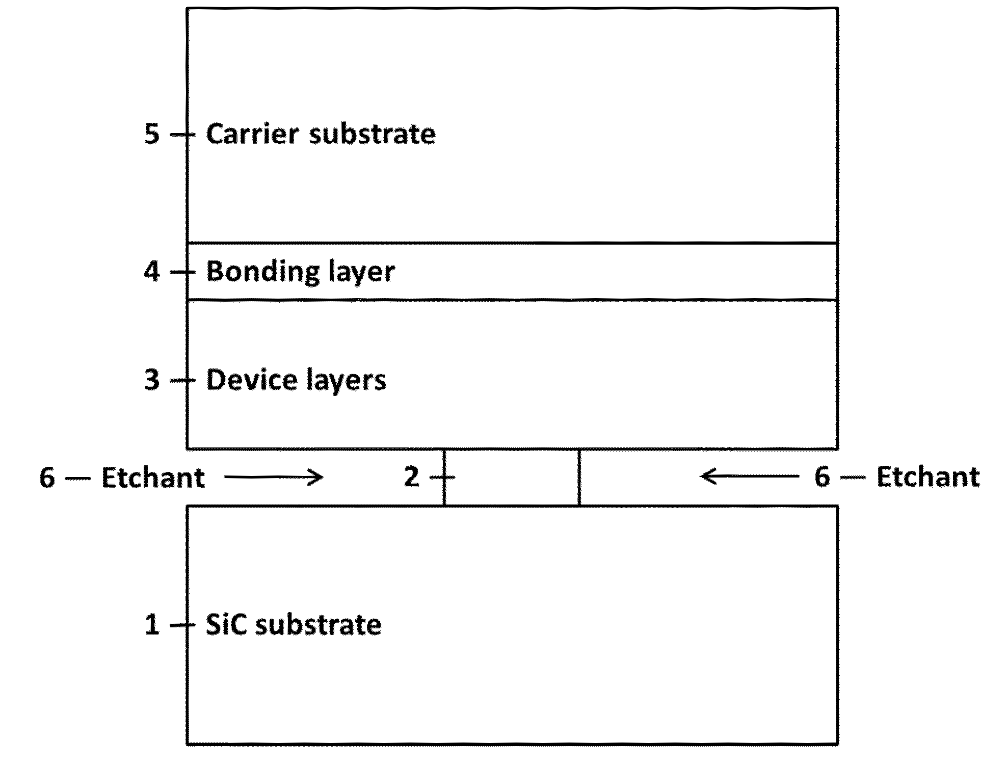
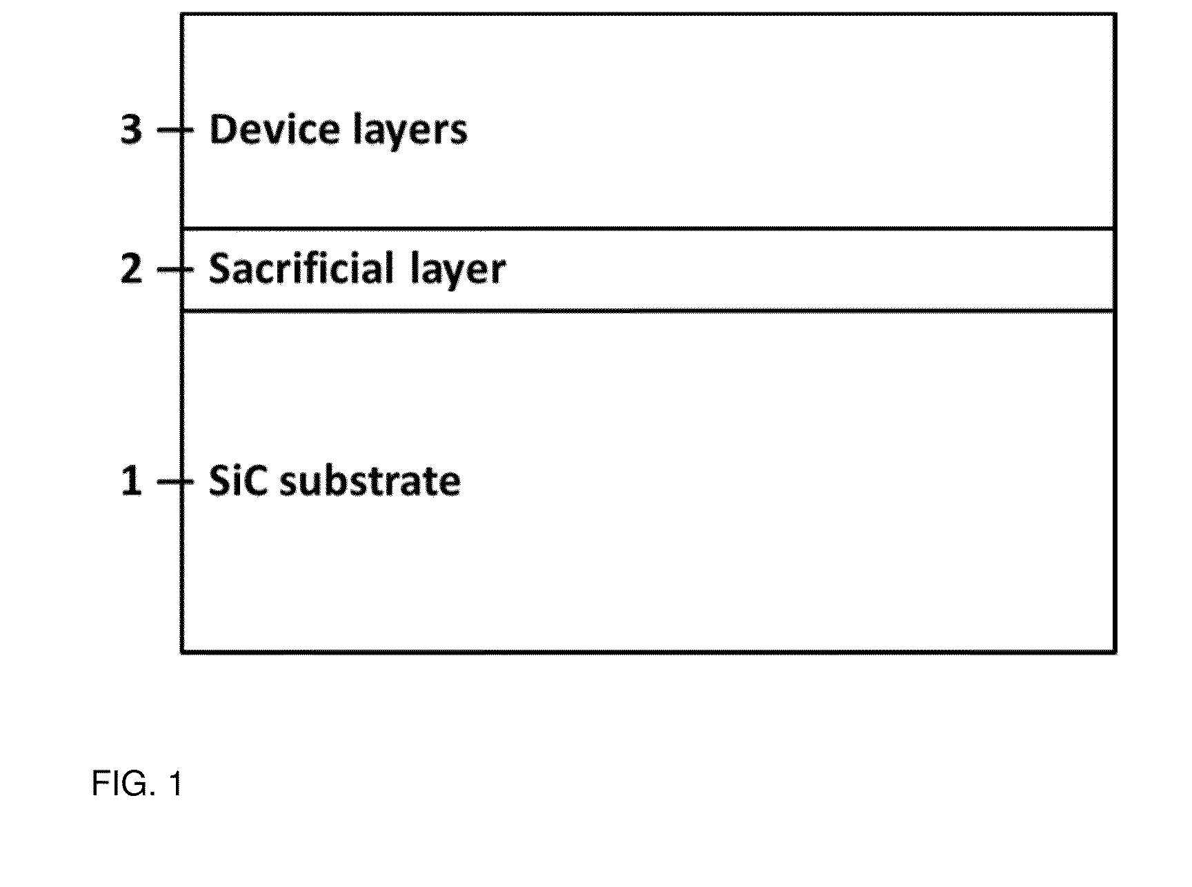
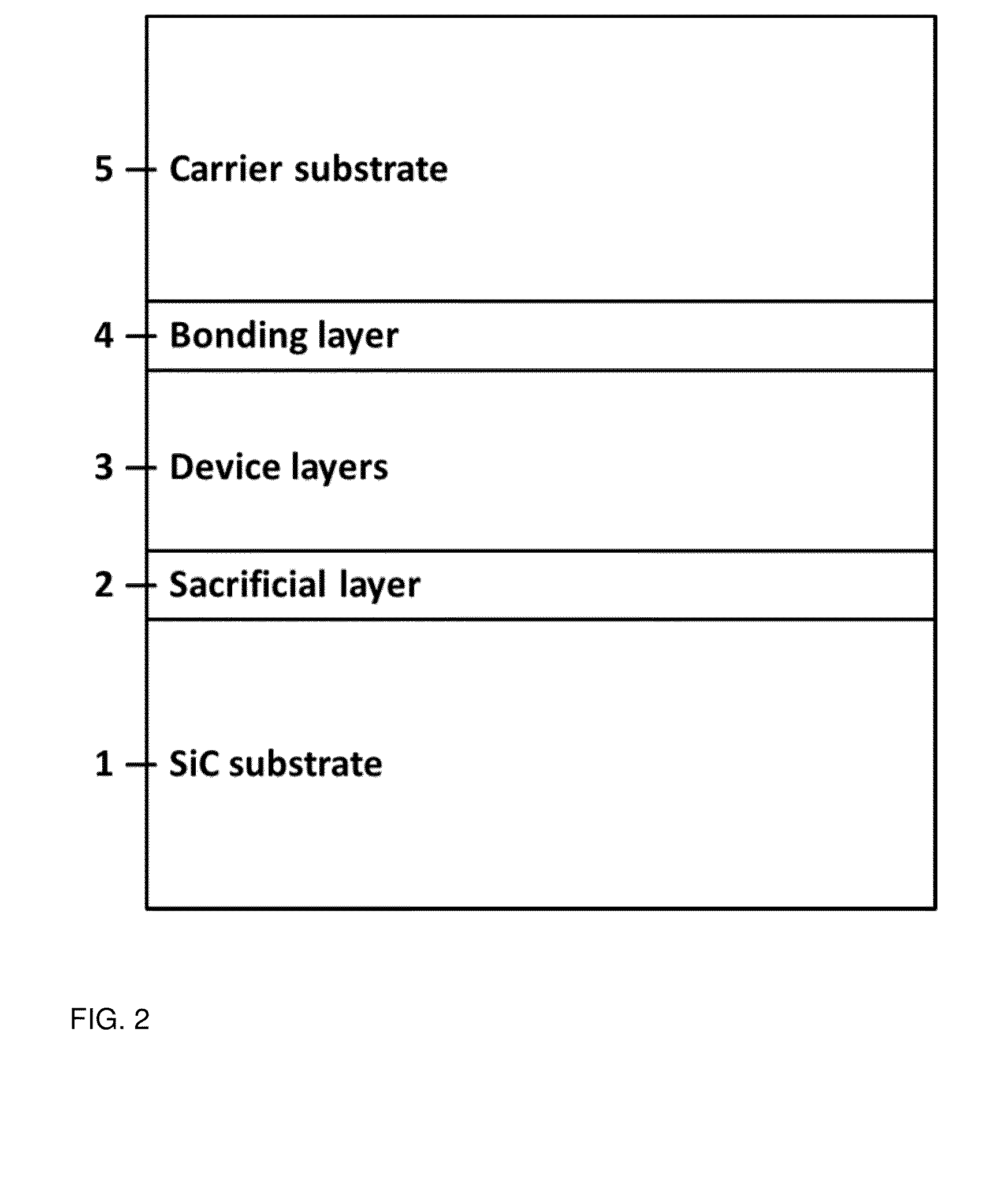
[0027]The present invention provides a process to remove epitaxially grown metal, semiconductor and / or insulator layers from a SiC substrate using an intermediate, sacrificial epitaxial layer. A preferred embodiment of this invention involves growing an epitaxial sacrificial layer 2 on the SiC substrate 1 prior to growing the remainder of the epitaxial device layers 3 as shown in FIG. 1. The SiC substrate should have a hexagonal crystal structure, consisting of either the 4H or 6H polytype. The sacrificial layer 2 should have a similar crystal structure and in-plane lattice constant, a, to SiC allowing for epitaxial growth of the sacrificial layer 2 on the SiC substrate 1. The sacrificial layer 2 should also be easily removed by selective etching compared to the SiC substrate 1 and any device layers 3 grown on top. The sacrificial layer 2 that has been experimentally demonstrated in our lab was tantalum nitride (Ta2N), but could also be other transition metal nitrides (TMN) such as ...


PUM


Abstract

A method to remove epitaxial semiconductor layers from a substrate by growing an epitaxial sacrificial layer on the substrate where the sacrificial layer is a transition metal nitride (TMN) or a TMN ternary compound, growing one or more epitaxial device layers on the sacrificial layer, and separating the device layers from the substrate by etching the sacrificial layer to completely remove the sacrificial layer without damaging or consuming the substrate or any device layer. Also disclosed are the related semiconductor materials made by this method.

Description

PRIORITY CLAIM[0001]The present application is a non-provisional application claiming the benefit of U.S. Provisional Application No. 61 / 846,687, filed on Jul. 16, 2013 by David J. Meyer et al., entitled “Lift-Off of Epitaxial Layers from silicon carbide or compound semiconductor substrates,” the entire contents of which is incorporated herein by reference.BACKGROUND OF THE INVENTION[0002]1. Field of the Invention[0003]The present invention relates to separating a semiconductor layer from a substrate.[0004]2. Description of the Prior Art[0005]SiC substrates are commonly used for the high quality growth of semiconductor materials such as the homoepitaxial growth of SiC or heteroepitaxial growth of Group III-Nitrides (III-Ns) including gallium nitride (GaN), aluminum nitride (AlN), indium nitride (InN), and their various alloys for electronic or optoelectronic applications. Although SiC substrates offer advantages such as close lattice matching to the III-N material system for high qu...

Claims


Application Information

Patent Timeline
IPC IPC(8): H01L29/16H01L29/20H01L21/762H01L21/306
CPCH01L21/30617H01L29/1608H01L29/2003H01L21/76256H01L21/32134H01L21/32135H01L21/6835H01L21/6836H01L21/7813H01L2221/68368H01L21/7806H01L2924/0002
Inventor MEYER, DAVID J.DOWNEY, BRIAN P.
Owner THE UNITED STATES OF AMERICA AS REPRESENTED BY THE SECRETARY OF THE NAVY
Why Eureka
Try Eureka