Touch sensing device and a detection method

a technology of touch sensing device and detection method, which is applied in the direction of resistance/reactance/impedence, instruments, and using reradiation, can solve the problems of high number of single sensing electrode elements, complicated manufacturing process as well as the measurement electronics of the touch sensing device, and user visibility of the touch sensitive film, etc., to achieve cost-effective implementation and increase the reliability of the device

Inactive Publication Date: 2015-01-22
CANATU OY
View PDF11 Cites 29 Cited by
  • Summary
  • Abstract
  • Description
  • Claims
  • Application Information

AI Technical Summary

Benefits of technology

[0065]In an embodiment, a 2- and 3-dimensional touch sensor devices are provided to applications whose enclosure cover has to be removed, for example to maintain and change the serviceable parts inside. It is also a robust method to provide data entry method to devices requiring unbroken encapsulation for, for example, wet, explosive or otherwise hazardous environments or where direct connection, as with interconnecting wires, is otherwise impossible, costly or highly inconvenient.
[0066]In an embodiment, no physical connector for power and data transmission that is susceptible to dirt, wear and tear or breakage. With no connector there are fewer parts susceptible to contamination, chemical or physical degradation o...

Problems solved by technology

One particularly challenging issue is the detection of multiple simultaneous touches which, on the other hand, often is one of the most desired properties of the state-of-the-art touch sensing devices.
Complex sensing electrode configurations and a high number of single sensing electrode elements complicates the manufacturing process as well as the measurement electronics of the touch sensing device.
Visibility of the touch sensitive film to the user of ...

Method used


Image

  • Touch sensing device and a detection method
  • Touch sensing device and a detection method
  • Touch sensing device and a detection method

Examples


Embodiment Construction

[0081]An explanation of the invention follows based on the examples described below.

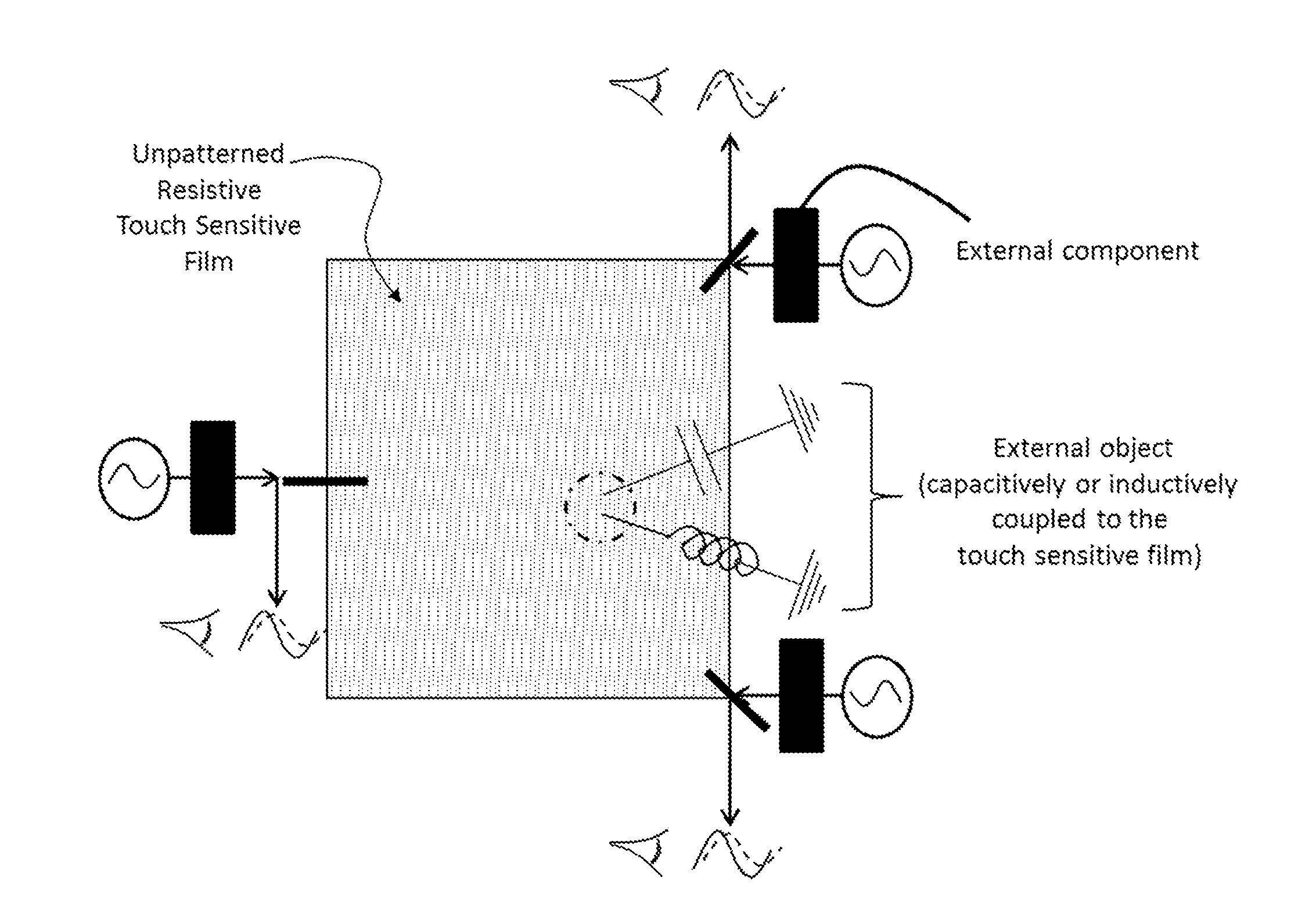
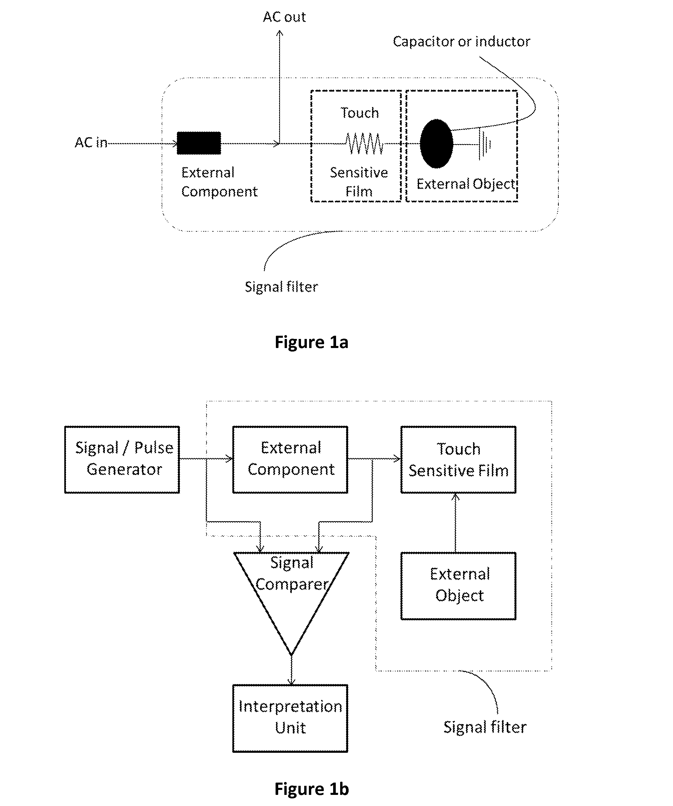
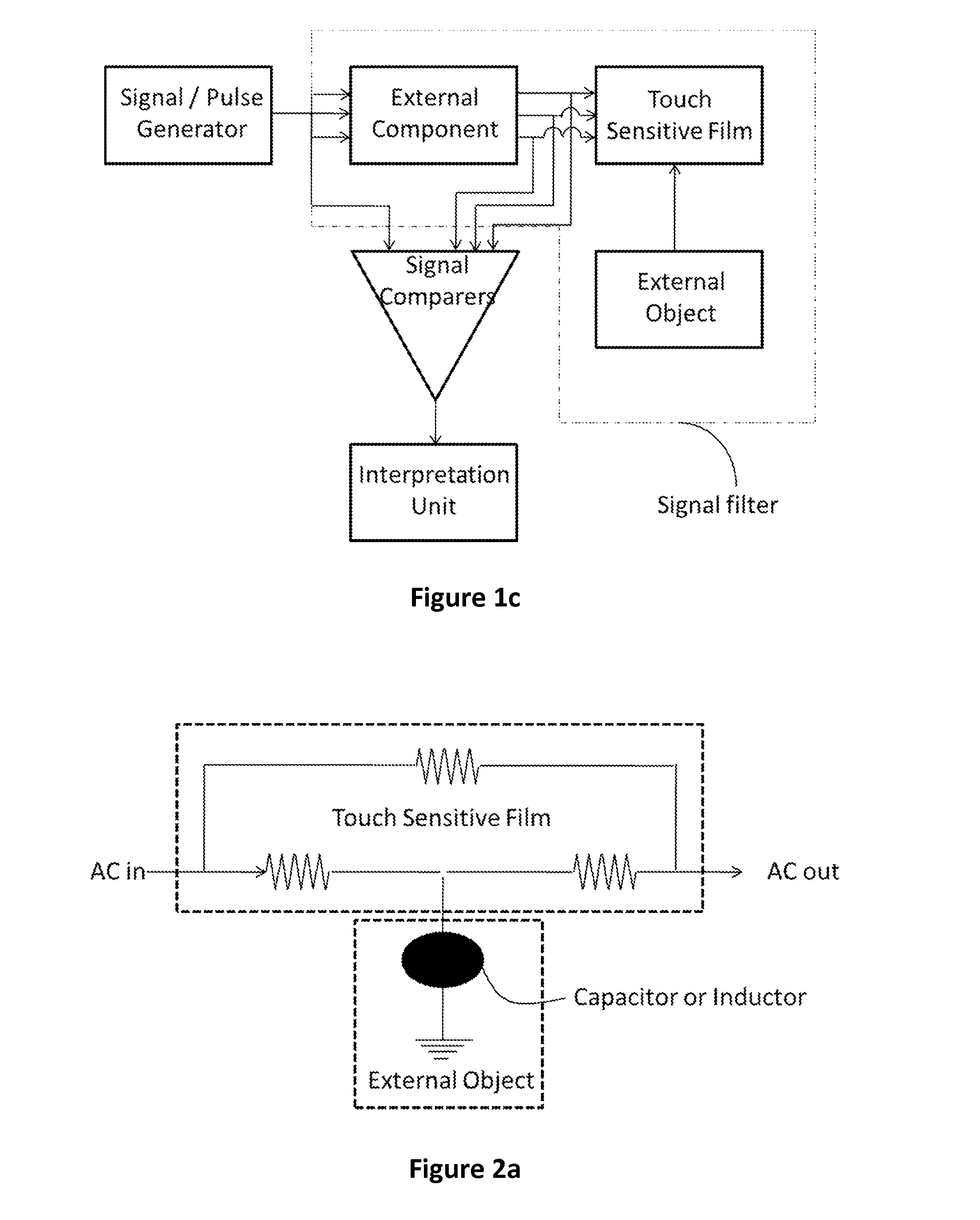
[0082]Capacitive or inductive coupling to an external object together with a resistive film compose an electronic signal filter. A touch sensitive film with sufficient electrical resistivity together with an external object having capacitance or inductance creates a low-pass RC filter due the resulting RC time constant of the system. The properties of this low-pass filter depend on the sheet resistance, as well as on location and capacitance or inductance of the external object.

[0083]In the typical operational mode, one or more oscillating signals or pulses are fed into the filter at one or more locations. In the touch sensitive film, the resistance between any two points on or at the edge of the touch surface is a function of their relative location and the geometry and sheet resistance of the sensor area. The capacitance or inductance in this system is a combination of parasitic capacitance or indu...


PUM


Abstract

A touch sensor having a touch sensitive film, a signal filter, electrical circuitry and a processing unit. The film is capable of capacitive or inductive coupling to an external object when a touch is made by the object. The signal filter is formed by the resistance of the film and the capacitive or inductive coupling to the external object, and the filter has properties affected by location of the touch and/or capacitance or inductance of the touch. The electrical circuitry is coupled to the touch sensitive film and configured to supply excitation, amplitude and wave form into the signal filter and to receive response signals from the signal filter. The processing unit is configured to detect the presence or proximity of a touch, the location of said touch, the capacitance and/or inductance of said touch by processing response signals and thereby measuring changes in the properties of the signal filter.

Description

FIELD OF THE INVENTION[0001]The present invention relates to touch sensing devices, more particularly to touch sensing devices having touch sensitive films, and to a method of detecting a touch and detecting its location.BACKGROUND OF THE INVENTION[0002]User interfaces for different kinds of electrical apparatuses are nowadays more and more often made with different types of touch sensing devices based on touch sensitive films instead of conventional mechanical buttons. Well known examples include different kinds of touch pads and touch screens in mobile phones, portable computers and similar devices. In addition to the sophisticated and even luxurious user experience achievable, touch sensing devices based on touch sensitive films also provide a superior freedom to the designers continuously trying to find functionally more versatile, smaller, cheaper, lighter, and also visually more attractive devices.[0003]A key element in such touch sensing devices is a touch sensitive film comp...

Claims


Application Information

Patent Timeline
IPC IPC(8): G01R27/26G01B7/00G06F3/044G01B7/14G01V3/00G01R27/02
CPCG01B7/14G06F3/044G01V3/00G01R27/02G01R27/2611G01B2210/58G01B7/003G06F2203/04104G06F2203/04112G06F2203/04102G01R27/2605G06F3/0416G06F3/046G06F3/016G06F3/0446G06F3/04166G06F3/0444G06F3/0443
Inventor RUUSUNEN, MATTI HANNUVON PFALER, JANMIKLADAL, BJORN FRIOURAITCHISON, BRADLEY J.BROWN, DAVID P.
Owner CANATU OY
Why Eureka
Try Eureka