Manufacturing method for liquid crystal display

a manufacturing method and liquid crystal technology, applied in the field of manufacturing methods for liquid crystal display panels, can solve the problems of insufficient display characteristics, increased complexity, size and cost of the manufacturing apparatus, and the inability to obtain liquid crystal display panels. achieve the effect of excellent display characteristics and high manufacturing efficiency

Inactive Publication Date: 2015-01-29
NITTO DENKO CORP
View PDF0 Cites 9 Cited by
  • Summary
  • Abstract
  • Description
  • Claims
  • Application Information

AI Technical Summary

Benefits of technology

[0024]According to one embodiment of the present invention, the polarizing plate having an absorption axis in its width direction and the reflective polarizing film are bonded before the slitting process is performed to prepare the optical film, and thus a directional relationship between the absorption axis of the polarizing film and the reflection axis of the reflective polarizing film can be precisely controlled. Besides, the optical film can be bonded onto a predetermined position on the liquid crystal cell by having been slit so as to have a predetermined width as described above, and by being conveyed while being positioned. Therefore, in the bonding of the optical film onto the liquid crystal cell, an axis direction can be satisfactorily controlled. As a result, high manufacturing efficiency can be realized with the use of the polarizing plate having an absorption axis in its width direction, and a liquid crystal display panel having extremely excellent display characteristics can be obtained.

Problems solved by technology

Consequently, there arises a problem in that a manufacturing apparatus is increased in complexity, size, and cost.
However, when the polarizing film having an absorption axis in its width direction is used, there arises a problem in that display characteristics of a liquid crystal display panel to be obtained are insufficient.

Method used


Image

  • Manufacturing method for liquid crystal display
  • Manufacturing method for liquid crystal display
  • Manufacturing method for liquid crystal display

Examples


Embodiment Construction

[0041]Hereinafter, preferred embodiments of the present invention are described with reference to the drawings. However, the present invention is not limited to these specific embodiments.

[0042]I. Manufacturing Method for Liquid Crystal Display Panel

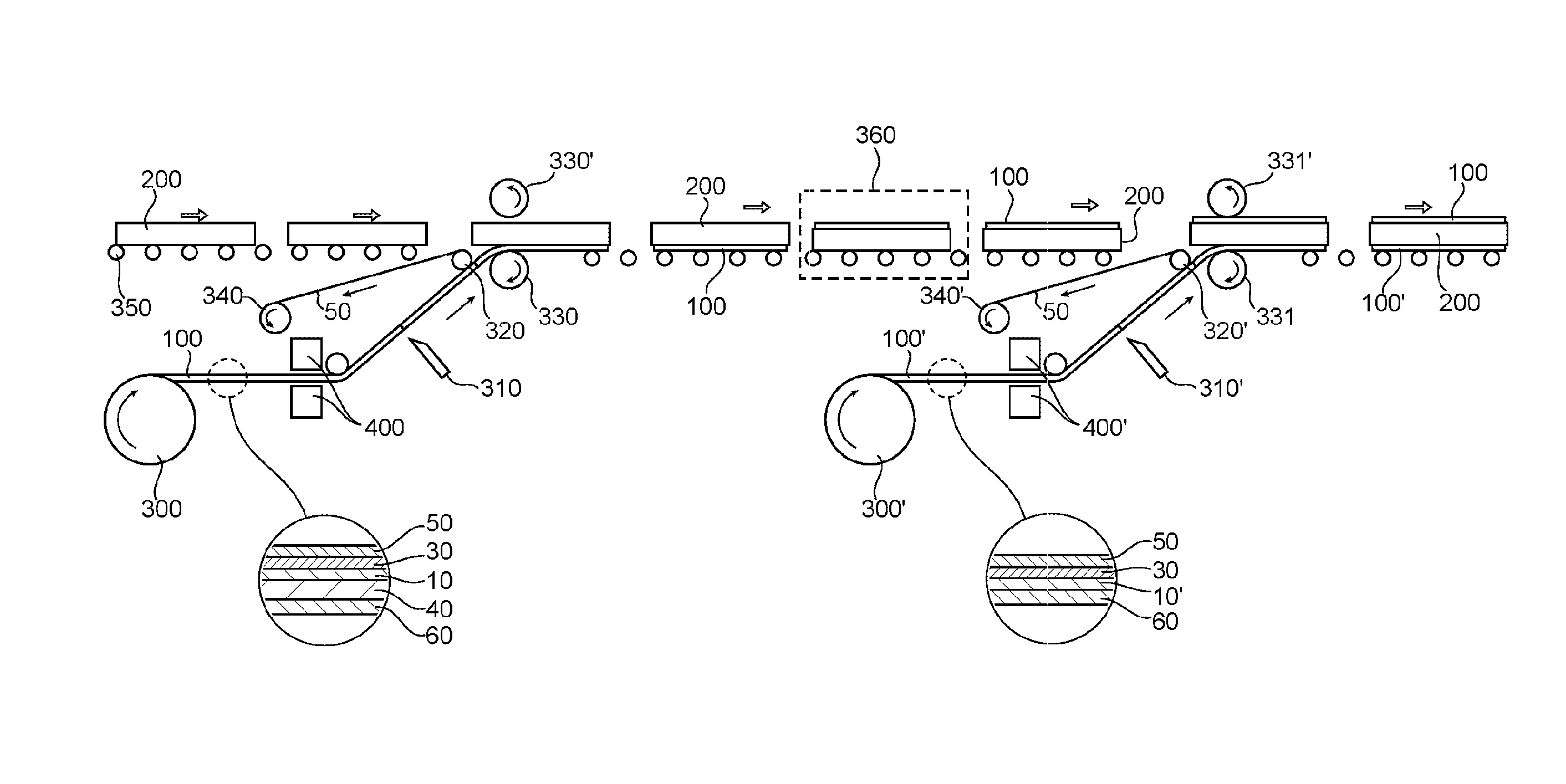
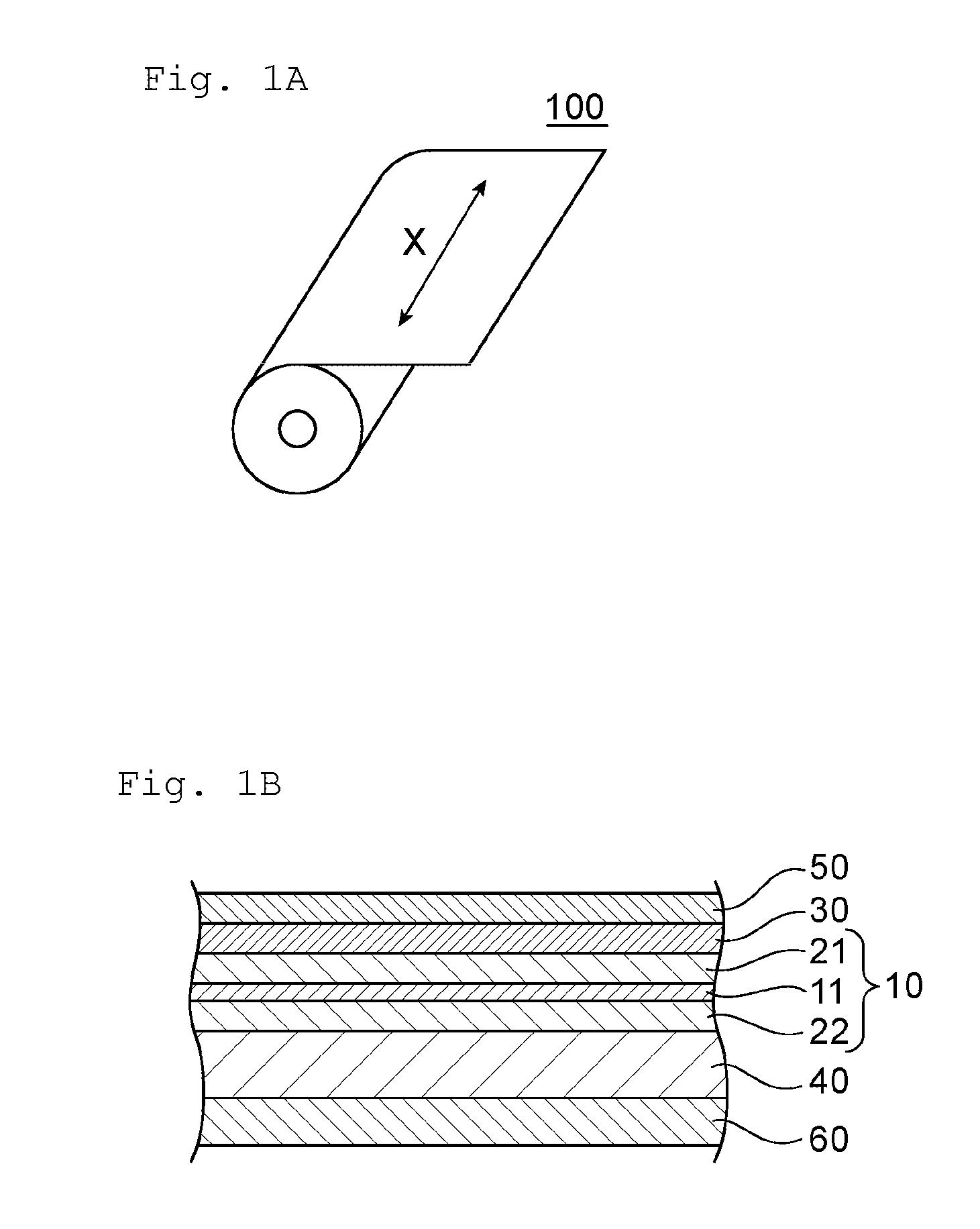
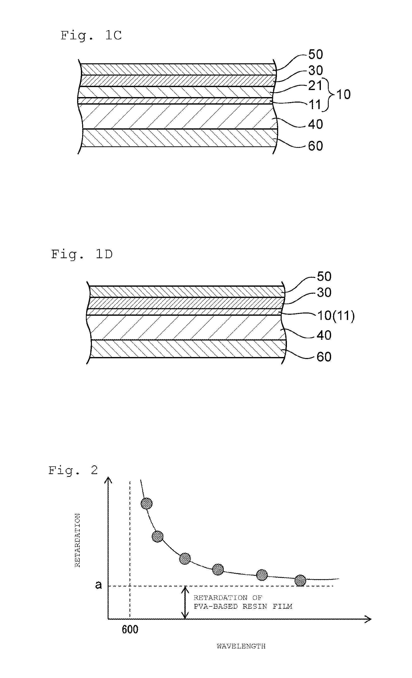
[0043]One embodiment of the present invention relates to a manufacturing method for a liquid crystal display panel. The liquid crystal display panel includes a liquid crystal cell and optical films arranged on both sides of the liquid crystal cell. The optical films each include a polarizing plate including a polarizing film. In the liquid crystal display panel, the polarizing films on both sides of the liquid crystal cell typically have absorption axes substantially perpendicular to each other. The manufacturing method according to the one embodiment of the present invention includes the steps of: cutting, while feeding a first optical film from an optical film roll, the optical film roll being obtained by slitting the first optical fil...


PUM

PropertyMeasurementUnit
thicknessaaaaaaaaaa
wavelength rangeaaaaaaaaaa
transmittanceaaaaaaaaaa

Abstract

A manufacturing method for a liquid crystal display panel includes slitting a first optical film having an elongate shape, to have a width corresponding to a pair of opposing sides of a liquid crystal cell, and by rolling the slit first optical film in its width direction to have a length corresponding to another pair of opposing sides of the liquid crystal cell; slitting a second optical film having an elongate shape, to have a width corresponding to a pair of opposing sides of the liquid crystal cell, and by rolling the slit second optical film in its width direction to have a length corresponding to another pair of opposing sides of the liquid crystal cell; bonding the cut first optical film onto one surface of the liquid crystal cell; and bonding the cut second optical film onto another surface of the liquid crystal cell.

Description

TECHNICAL FIELD[0001]The present invention relates to a manufacturing method for a liquid crystal display panel.BACKGROUND ART[0002]There are many proposals concerning a method involving, in a manufacturing line for a liquid crystal display panel, cutting a roll-shaped optical film while feeding the optical film to attach the optical film to a liquid crystal cell (so-called roll-to-panel; RTP) (for example, Patent Literature 1). For example, in Patent Literature 1, there is a disclosure of a method involving: while feeding a long optical film from an optical film roll, cutting the optical film to a length corresponding to a long side of a liquid crystal cell to attach the optical film to one surface of the liquid crystal cell, the optical film roll being obtained by winding a long optical film that includes a polarizing film having an absorption axis in its longitudinal direction and has been subjected to cutting (slitting process) to a width corresponding to a short side of the liq...

Claims


Application Information

Patent Timeline
Patent Type & Authority Applications(United States)
IPC IPC(8): G02F1/1333G02F1/13B29C65/72G02F1/1335
CPCG02F1/133351G02F1/133536G02F1/1303B29D11/0073G02F2001/133562G02F2001/133567B29C65/72B32B38/0004B32B38/0008B32B2038/0028B32B2038/045B32B2309/105B32B2327/00B32B2457/202B32B37/185Y10T156/1074Y10T156/1335G02F1/133562G02F1/133567
Inventor HADA, KAZUYAKONDO, SEIJIHIRATA, SATOSHI
Owner NITTO DENKO CORP
Why Eureka
Try Eureka