Transparent conductive film, substrate carrying transparent conductive film, and production method thereof

a technology of transparent conductive film and substrate, which is applied in the direction of removing conductive materials by irradiation, instruments, nuclear engineering, etc., can solve the problems of increasing energy consumption for the preparation of insulation pattern layer, and the method described in patent document 1 is not suited for large-area conductive nanofiber sheets, etc., to reduce the aspect ratio of metal nanowires, reduce the number of contact points, and convert electrically conductive regions

Inactive Publication Date: 2015-01-29
PANASONIC INTELLECTUAL PROPERTY MANAGEMENT CO LTD
View PDF1 Cites 28 Cited by
  • Summary
  • Abstract
  • Description
  • Claims
  • Application Information

AI Technical Summary

Benefits of technology

[0023]According to the present invention, when irradiated with light or heated, the insulator-conversion promoting component decomposes metal nanowires or reduces the aspect ratio of the metal nanowires, thereby reducing the number of contact points between metal nano

Problems solved by technology

However, the method described in Patent Document 1, which fuses and breaks the conductive nanofibers thermally by direct irradiation of the conductive nanofibers with the high-energy ray, needs more time to prepare the patterned insulating layer and causes an increase in

Method used


Image

  • Transparent conductive film, substrate carrying transparent conductive film, and production method thereof
  • Transparent conductive film, substrate carrying transparent conductive film, and production method thereof
  • Transparent conductive film, substrate carrying transparent conductive film, and production method thereof

Examples


example 1

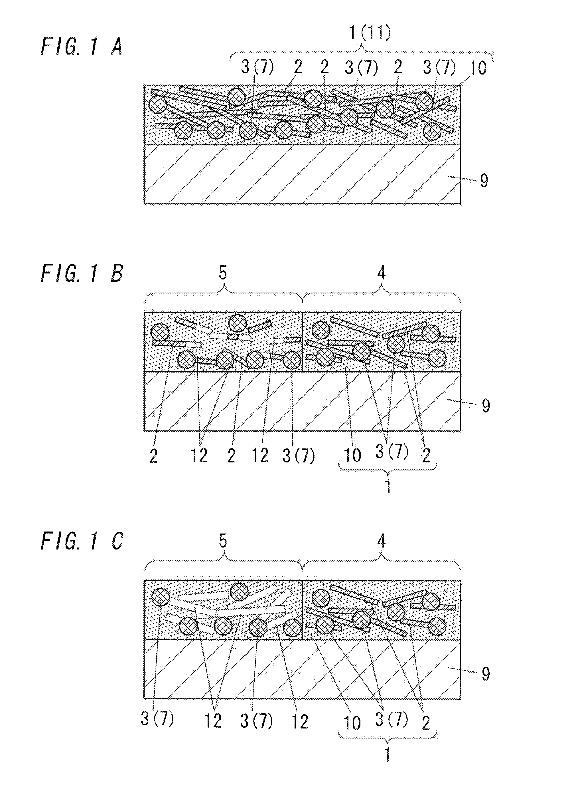
[0070]The transparent substrate 9 used was a non-alkali glass plate (“No. 1737”, refractive index at a wavelength of 500 nm: 1.50 to 1.53, available from Corning Inc.). The transparent conductive material A was applied on the surface of the transparent substrate by spin coating method and heated for drying and hardening under the condition of 100° C. and 5 minutes, to give a transparent conductive film having a film thickness of 100 nm. Then, to form an electrically insulating region, a light having an average energy density of 0.5 J / cm2 was emitted to the left half of the transparent conductive film by means of a UV-YAG laser. Thus, a substrate carrying the transparent conductive film having an electrically conductive region in the right half of the transparent conductive film and an electrically insulating region in the left half thereof was prepared.

example 2

[0071]A transparent conductive film having a film thickness of 100 nm was prepared in a manner similar to Example 1, except that the transparent conductive material A was replaced with the transparent conductive material B. Then, an electrically insulating region was formed similarly to Example 1, to give a substrate carrying the transparent conductive film having an electrically conductive region in the right half of the transparent conductive film and an electrically insulating region in the left half thereof.

example 3

[0072]A transparent conductive film having a film thickness of 100 nm was prepared in a manner similar to Example 1, except that the transparent conductive material A was replaced with the transparent conductive material C. Then, an electrically insulating region was formed similarly to Example 1, to give a substrate carrying the transparent conductive film having an electrically conductive region in the right half of the transparent conductive film and an electrically insulating region in the left half thereof.


PUM


Abstract

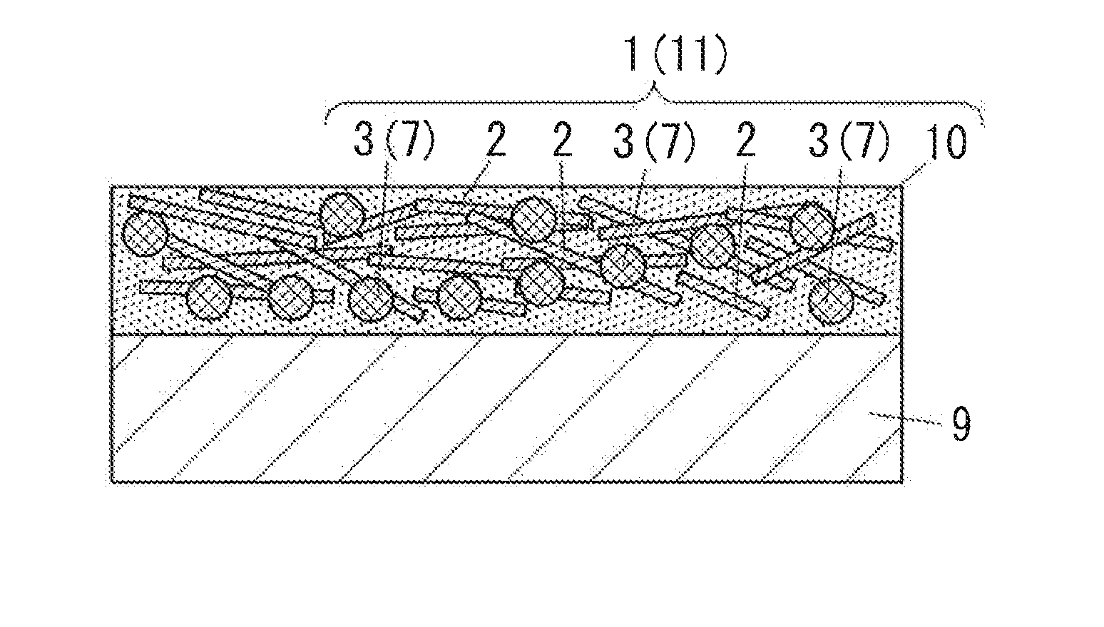
Provided is a transparent conductive film wherein an electrically conductive region is converted to an electrically insulating region more readily and rapidly than traditional conductive films and the level difference between the electrically conductive region and the electrically insulating region is smaller. The transparent conductive film has an electrically conductive region 4 and an electrically insulating region 5. The electrically conductive region 4 contains a resin component 10, a metal nanowire 2 and an insulation-promoting component 3. The insulation-promoting component 3 has a light absorption higher than that of the metal nanowire 2. The electrically insulating region 5 is defined by a region which contains a resin component 10 but not the metal nanowire 2 or a region which contains a resin component 10 and additionally a metal nanowire 2 having an aspect ratio of smaller than that of the metal nanowire 2.

Description

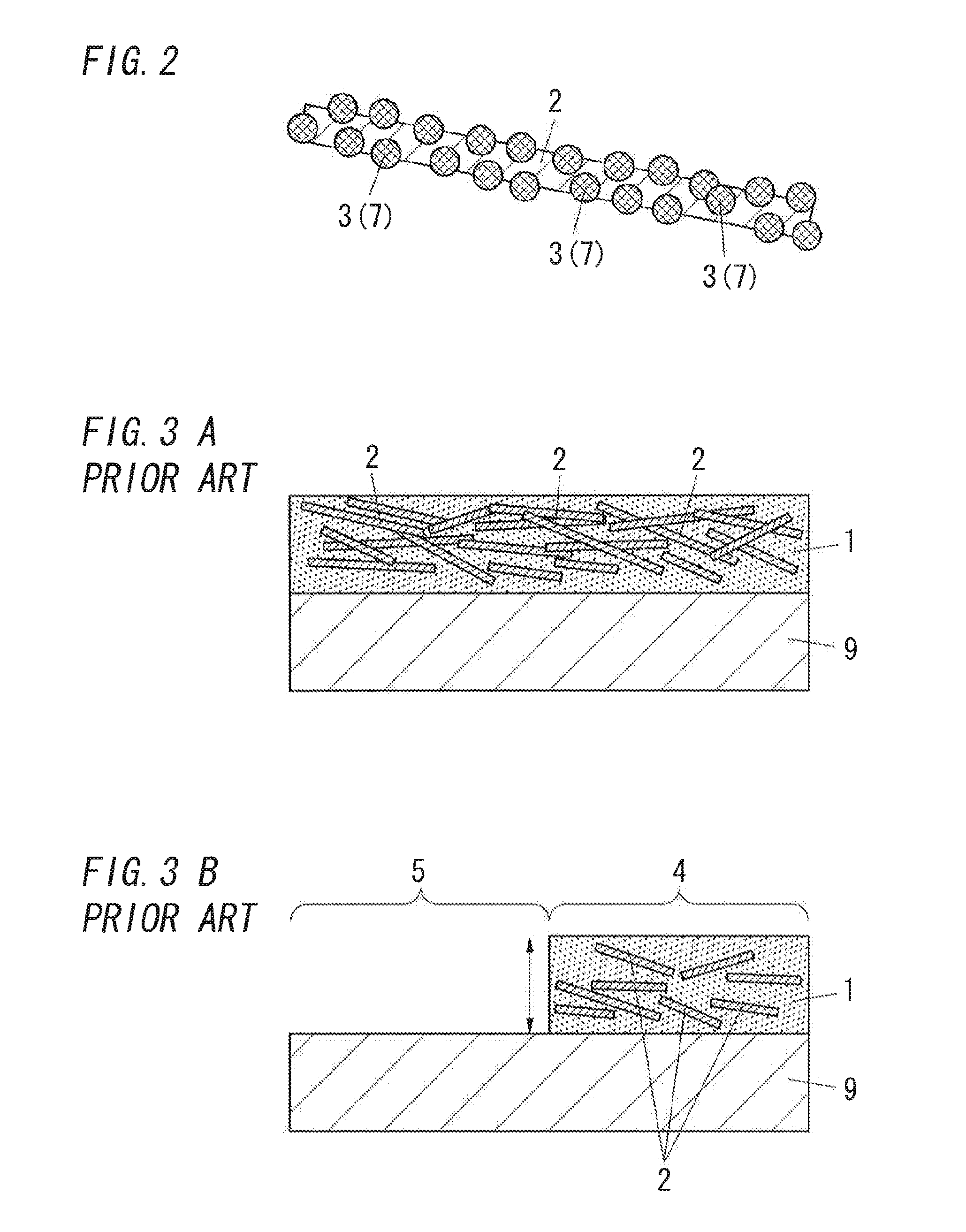
TECHNICAL FIELD[0001]The present invention relates to a transparent conductive film for use in various devices including touch panels, a substrate carrying the transparent conductive film, and a production method thereof.BACKGROUND ART[0002]Transparent conductive films have been used widely in touch panels, organic EL devices, liquid crystal displays, solar cells, and other devices. For example, an ITO film as transparent conductive film is formed by sputtering on the surface of a transparent substrate, and transparent electrodes are produced by patterning (pattern formation) on the ITO film by photoetching. In addition as shown in FIG. 3A, a transparent conductive film 1 containing metal nanowires 2 is formed on the surface of a transparent substrate 9, and the undesirable regions thereof are removed by photoetching or laser beam machining, to produce transparent electrodes constituted by the preserved electrically conductive regions 4, as shown in FIG. 3B. Further, as shown in FIG...

Claims


Application Information

Patent Timeline
IPC IPC(8): H05K1/02H05K3/46H05K3/02H05K1/03H05K1/09
CPCH05K1/0274H05K1/0313H05K1/097H05K2201/2054H05K3/4664H05K2201/032H05K3/027B82Y30/00G06F3/041G06F2203/04103C09D101/02
Inventor TSUJIMOTO, AKIRATADAMASA, AKIHIKOMATSUI, TAISUKEYASUHARA, ERI
Owner PANASONIC INTELLECTUAL PROPERTY MANAGEMENT CO LTD
Why Eureka
Try Eureka